
Inductively coupled antenna and plasma processing apparatus using the same
a plasma processing and inductive coupling technology, applied in the direction of plasma technique, chemical vapor deposition coating, coating, etc., can solve the problems of increasing the kinetic energy of ions, adversely affecting each other, and insufficient plasma density distribution in the reaction chamber b>10/b>, so as to improve the uniformity of plasma, reduce damage to a substrate, and reduce capacitive coupling.
Patent Information
- Authority / Receiving Office
- US · United States
- Patent Type
- Patents(United States)
- Current Assignee / Owner
- Publication Date
- 2010-06-22
- Estimated Expiration
- Not applicable · inactive patent
Smart Images
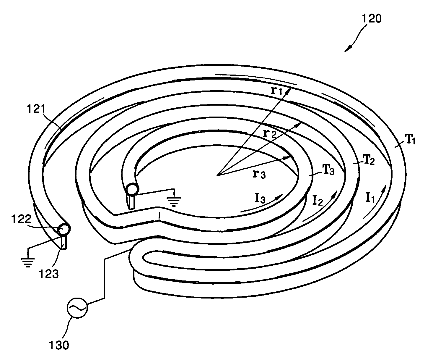
Figure 1 
Figure 2 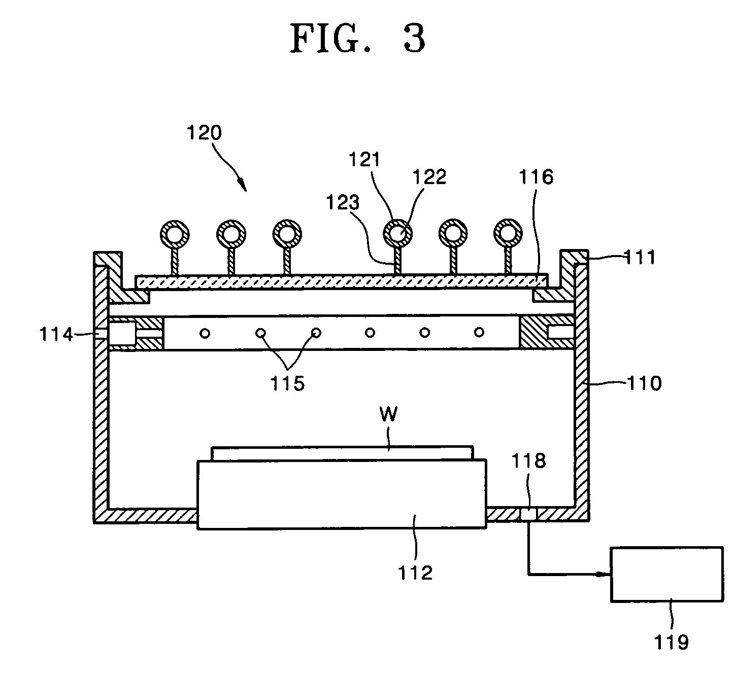
Figure 3
Abstract
Description
BACKGROUND OF THE INVENTION
[0001] 1. Field of the Invention
[0002] The present invention relates to an inductively coupled plasma processing apparatus. More particularly, the present invention relates to an inductively coupled antenna having a structure for improving plasma uniformity, and a plasma processing apparatus using the same.
[0003] 2. Description of the Related Art
[0004] Recently, plasma techniques have been widely used in fine processing of substrates during the fabrication of semiconductor devices or flat display panels. In those techniques, plasma is used to etch or deposit predetermined material layers on the surfaces of wafers for fabricating semiconductor devices or on the surfaces of substrates for fabricating liquid crystal displays (LCD). In particular, plasma processing apparatuses have been increasingly used to etch or deposit thin layers on substrates for fabricating highly integrated semiconductor devices.
[0005] Examples of plasma processing apparatuses used when fab...
Examples
first embodiment
[0030]FIG. 3 illustrates a sectional view of a structure of an inductively coupled plasma (ICP) processing apparatus having an antenna according to the present invention. FIG. 4 illustrates a perspective view of the antenna shown in FIG. 3.
[0031]Referring to FIGS. 3 and 4, an ICP processing apparatus according to a first embodiment of the present invention is used to perform fine processes. These fine processes include etching the surfaces of semiconductor device substrates, for example, wafers W, or depositing predetermined material layers on the surfaces of the wafers W, using plasma that is generated by an antenna 120.
[0032]The ICP processing apparatus includes a reaction chamber 110 having a plasma forming space therein. The inside of the reaction chamber 110 is maintained in a vacuum state using a vacuum suction port 118 that is formed on a bottom of the reaction chamber and connected to a vacuum pump 119. An electrostatic chuck 112 for supporting a substrate, for example, a wa...
second embodiment
[0046]FIG. 5 illustrates a sectional view of a structure of an ICP processing apparatus having an antenna according to the present invention. As mentioned above, the same reference numerals used in FIG. 3 denote the same elements.
[0047]An antenna 220 according to the second embodiment of the present invention includes a conductive metal tube 221 having a cooling path 222 and a conductive metal strip 223 that is electrically and thermally connected to a lower portion of the metal tube 221. In addition, a height of the metal strip 223 gradually decreases from a center portion to an edge portion of the antenna 220. According to the structure of the antenna in the second embodiment of the present invention, the strength of an electric field induced at the edge portion of the antenna 220 is enhanced so that the density of the plasma increases at the edge portion of the antenna 220. Thus, the density distribution of plasma in the reaction chamber 110 becomes uniform.
[0048]In the case of a...