
Method of manufacturing dual gate oxide devices
a technology of oxide devices and oxide layers, applied in the direction of semiconductor devices, basic electric elements, electrical apparatus, etc., can solve the problems of photoresist residue, process defects, and photoresist residue, and achieve the effects of improving the density of photoresist, reducing the risk of photoresist defects, and improving the resistance to acid solutions
Patent Information
- Authority / Receiving Office
- US · United States
- Patent Type
- Patents(United States)
- Current Assignee / Owner
- Publication Date
- 2015-02-24
Smart Images
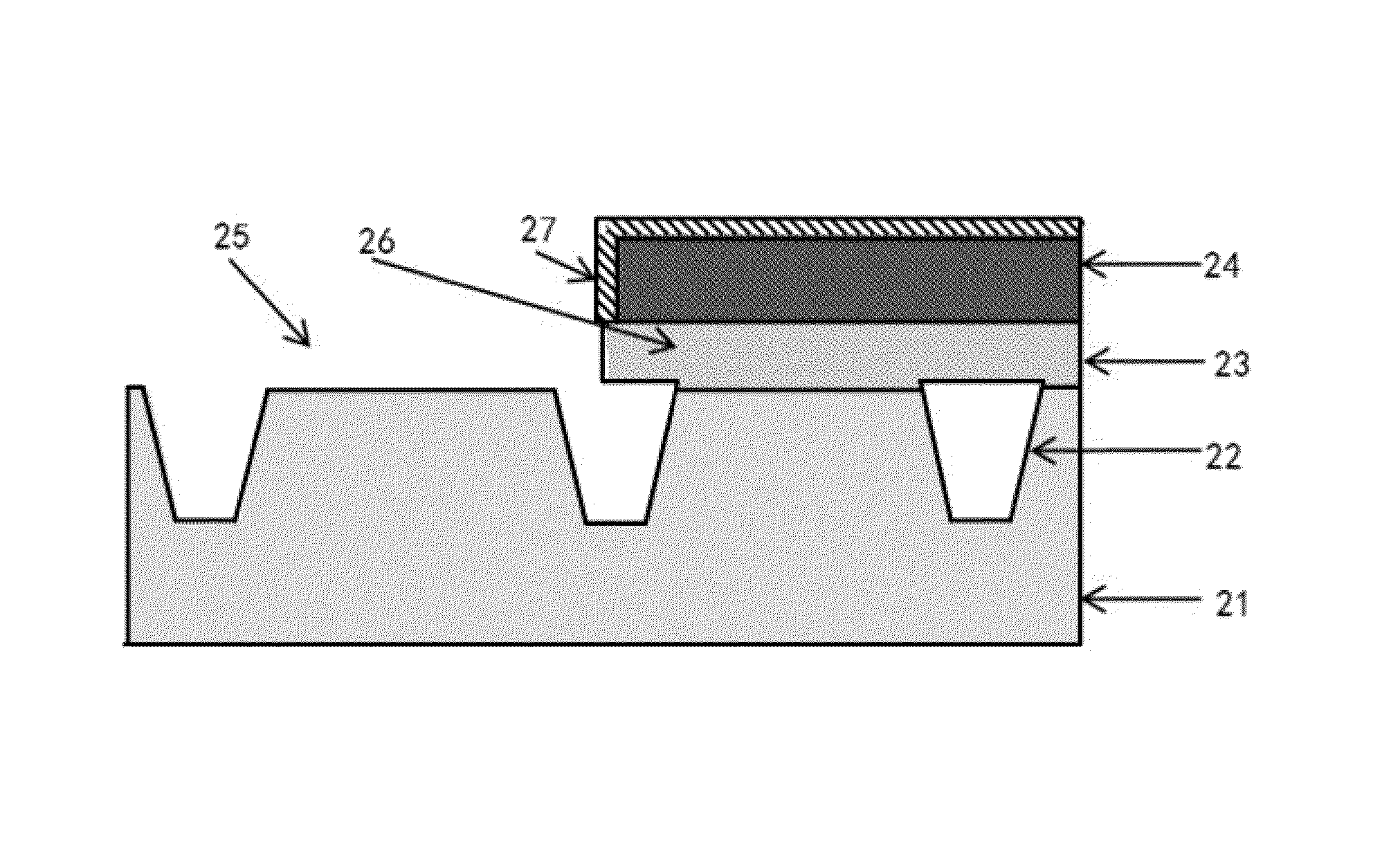
Figure 1 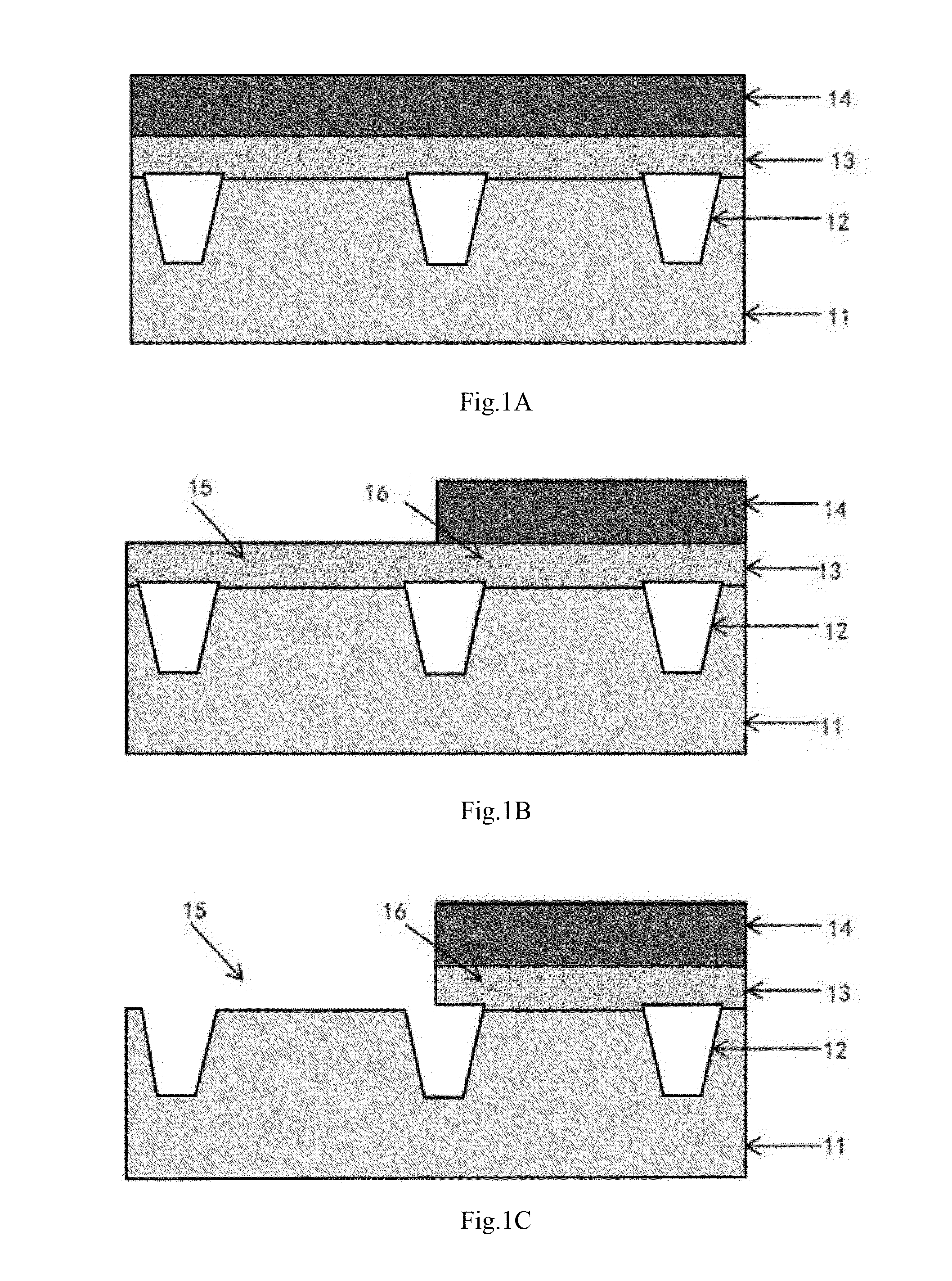
Figure 2 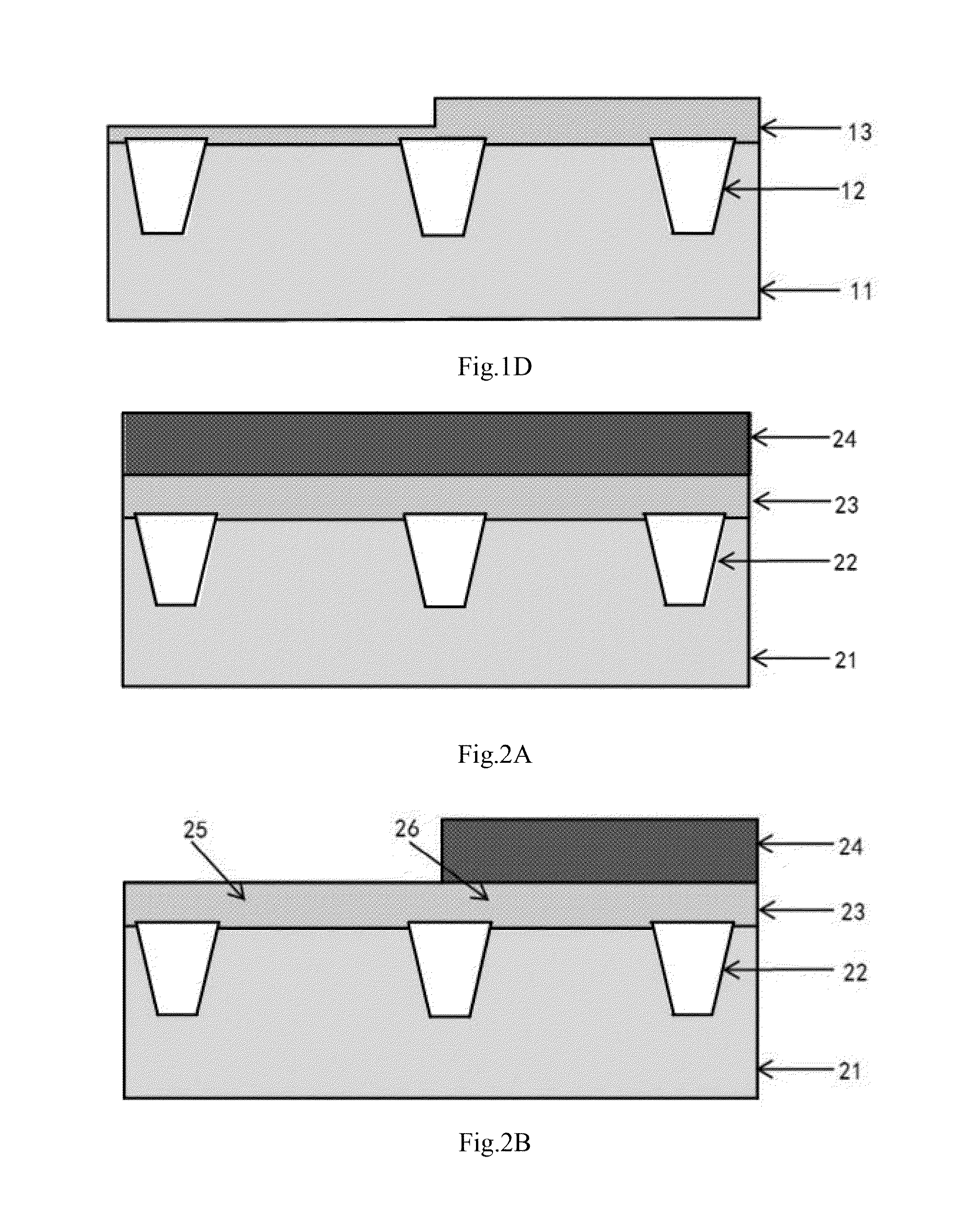
Figure 3
Abstract
Description
CROSS-REFERENCE TO RELATED APPLICATION
[0001] This application claims the priority benefit of China application serial no. 201310177577.5, filed May 14, 2013. All disclosure of the China application is incorporated herein by reference.FIELD OF THE INVENTION
[0002] The present invention relates to the field of semiconductor fabrication technology and particularly to a method of manufacturing dual gate oxide devices.BACKGROUND OF THE INVENTION
[0003] With the development of semiconductor technology, one integrated circuit (IC) chip will integrate pluralities of functional devices, which comprise different Field Effect Transistors (FETs) respectively. The multiple gate oxide process has become a common method to form different FETs in a same chip.
[0004] Nowadays, varieties of multiple gate oxide processes are provided. FIG. 1A to FIG. 1D show cross-sectional views of a dual gate oxide device in the conventional manufacturing process. As shown in FIG. 1A, the silicon substrate 11 with shallow ...
Examples
Embodiment Construction
[0029]The method of manufacturing dual gate oxide devices of the present invention will be described in further details hereinafter with respect to the embodiments and the accompanying drawings.
[0030]The present invention is described with reference to the attached figures, wherein like reference numerals are used throughout the figures to designate similar or equivalent elements. The figures are not drawn to scale and they are provided merely to illustrate the invention. It should be understood that numerous specific details, relationships, and methods are set forth to provide an understanding of the invention. One skilled in the relevant art, however, will readily recognize that the invention can be practiced without one or more of the specific details or with other methods. In other instances, well-known structures or operations are not shown in detail to avoid obscuring the invention.
[0031]Referring to FIG. 2A to FIG. 2E, in one embodiment of the present invention, the method of...