
Semiconductor device with multiple carrier channels
Patent Information
- Authority / Receiving Office
- US · United States
- Current Assignee / Owner
- Publication Date
- 2016-08-16
Smart Images
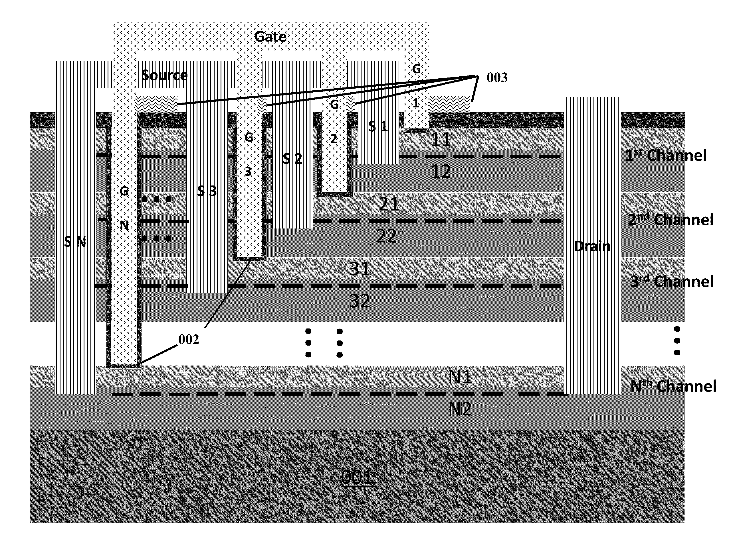
Figure 1 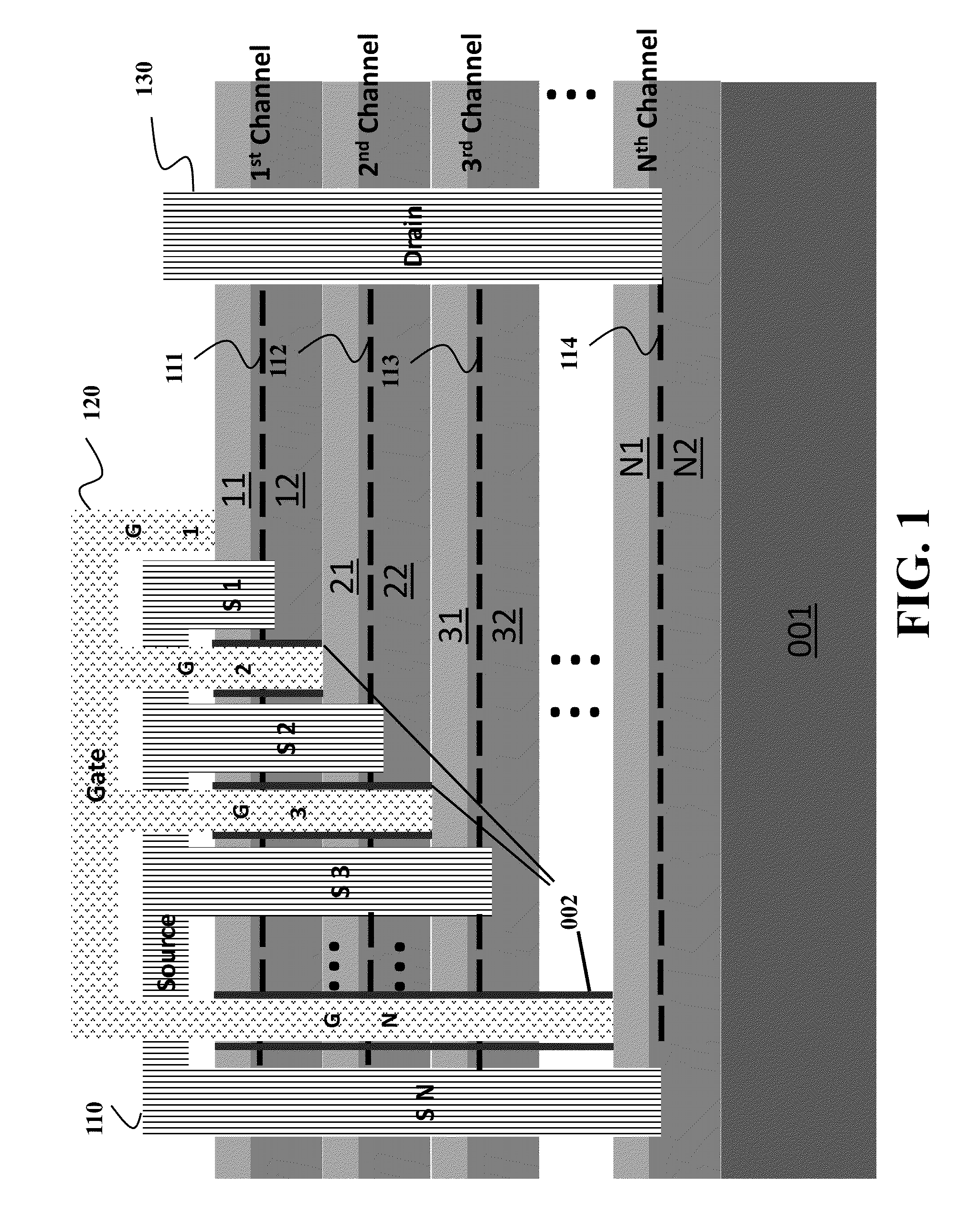
Figure 2 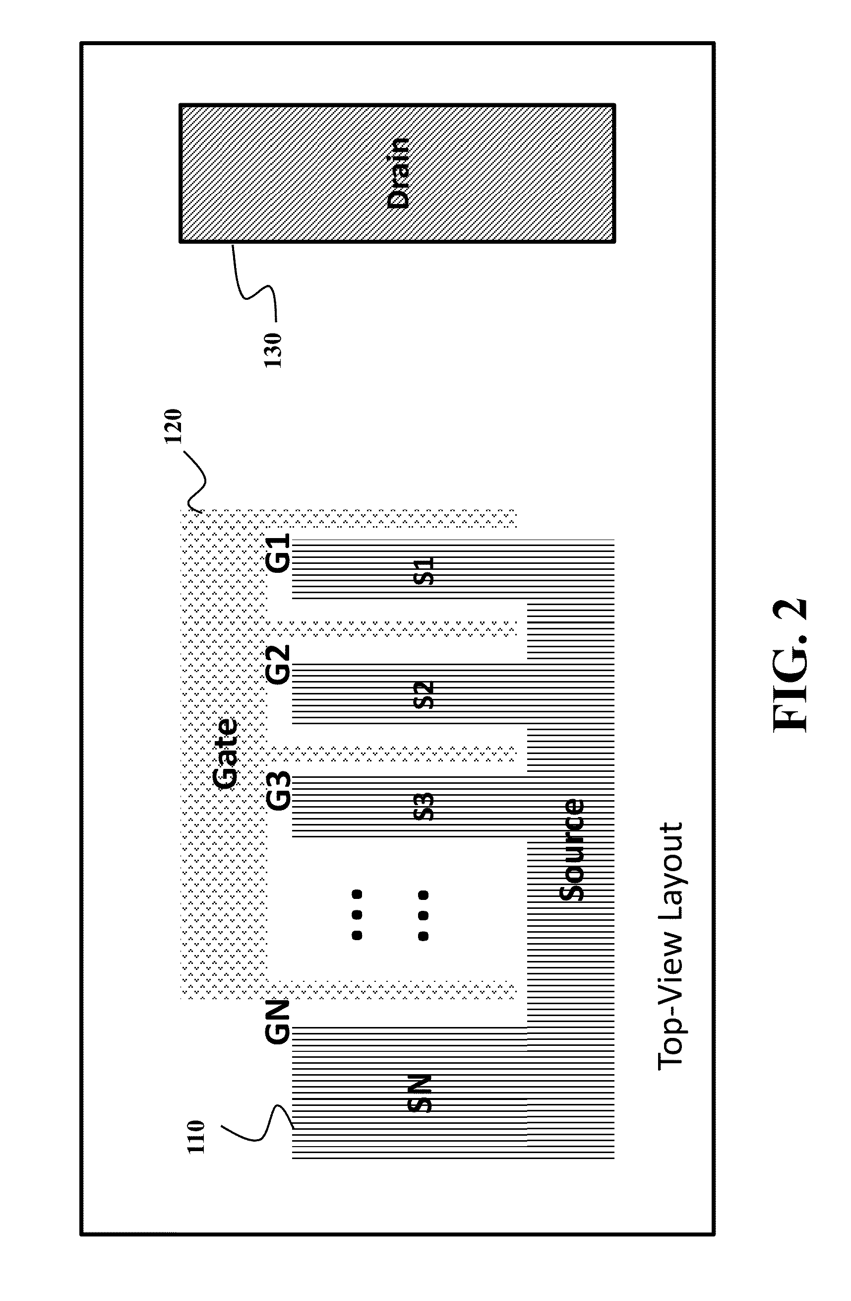
Figure 3
Abstract
Description
RELATED APPLICATION
[0001] This application claims priority from a provisional application 62 / 193,673 filed on Jul. 17, 2015 and incorporated herein by reference.FIELD OF THE INVENTION
[0002] The present invention relates generally to semiconductor device, and more particularly to semiconductor devices with multiple carrier channels.BACKGROUND OF THE INVENTION
[0003] Semiconductor devices play a significant role in solving the energy challenges. Specifically, nitride power transistors have great potential in the application of advanced transportation systems, more robust energy delivery networks and many new revolutionary approaches to high-efficiency electricity generation and conversion. Those systems rely on very efficient converters to step-up or step-down electric voltages. Nowadays, these devices are mainly made of silicon (Si). However, the limited breakdown voltage and frequency response of Si, and its higher resistance make the commercial devices and circuits currently available ...
Examples
Embodiment Construction
[0023]Various embodiments of the invention relates to a semiconductor device with multi-channels structure and an electrode controlling the multi-channels, and the methods and techniques for fabricating the device. Merely by way of example, different embodiments can be applied to methods and systems for manufacturing semiconductor devices with multiple two-dimensional-electron (2DEG) channels and / or two-dimensional-hole (2DHG) channels. The methods and techniques can be applied to a variety of three-terminal semiconductor devices, including but not limiting to bipolar transistors, field-effect transistor, insulated-gate bipolar transistors (IGBTs), and thyristors to enable the control over multi-channels in the device. The principles employ by some embodiments of the invention can be also used to form and / or fabricate the multi-channel field effect transistor (FET).
[0024]FIG. 1 shows a simplified cross-sectional diagram of a semiconductor device according to one embodiment of the in...