
Systems, methods, and apparatus for minimizing cross coupled wafer surface potentials
a technology of cross-coupling potential and system, applied in the field of wafer processing, can solve the problems of difficult, if not impossible, direct or contact measurement, etc., and achieve the effect of minimizing rf cross-coupling, minimizing rf power to the substrate, and minimizing the cross-coupling of rf power
Patent Information
- Authority / Receiving Office
- US · United States
- Patent Type
- Patents(United States)
- Current Assignee / Owner
- Publication Date
- 2017-03-07
Smart Images
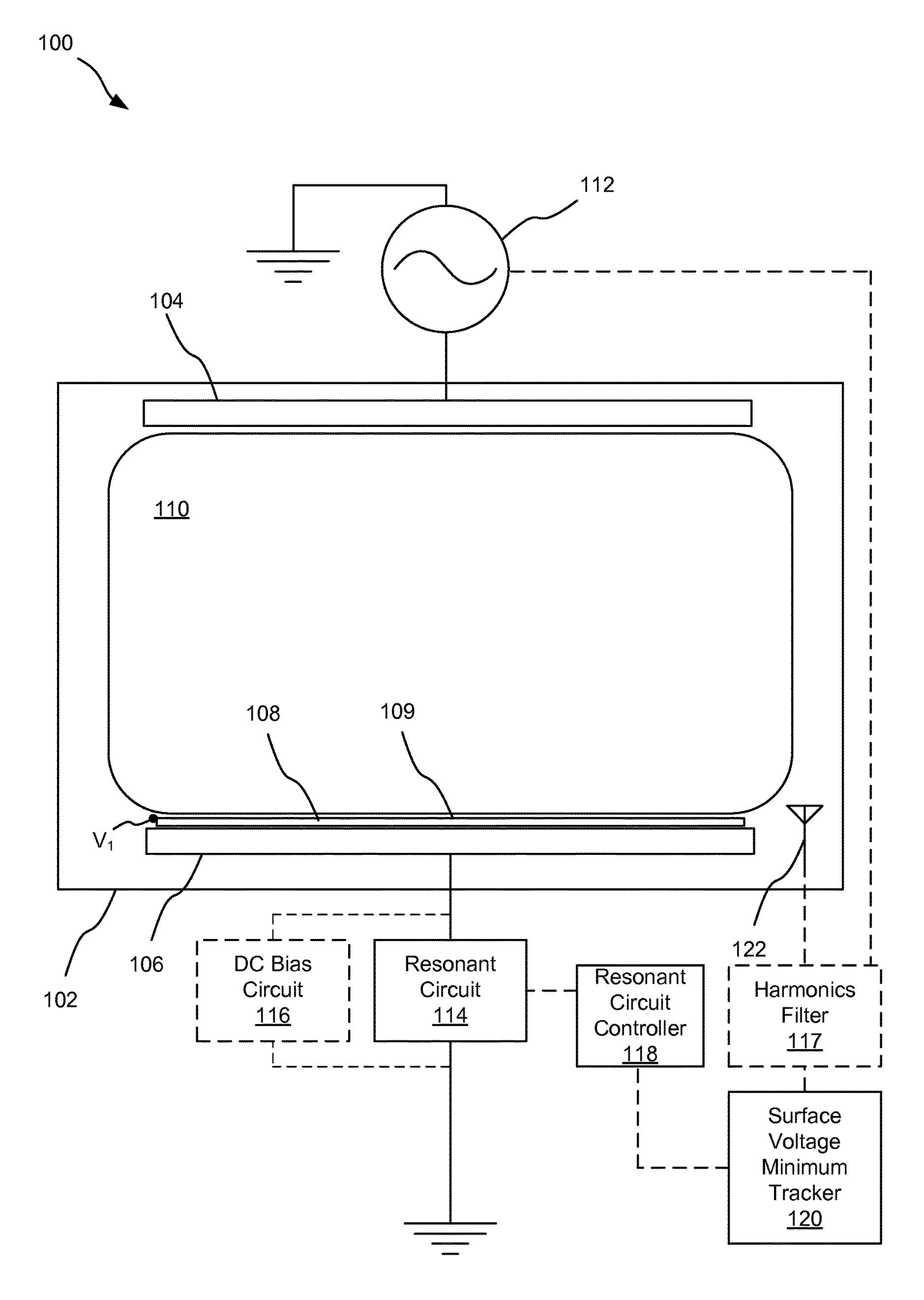
Figure 1 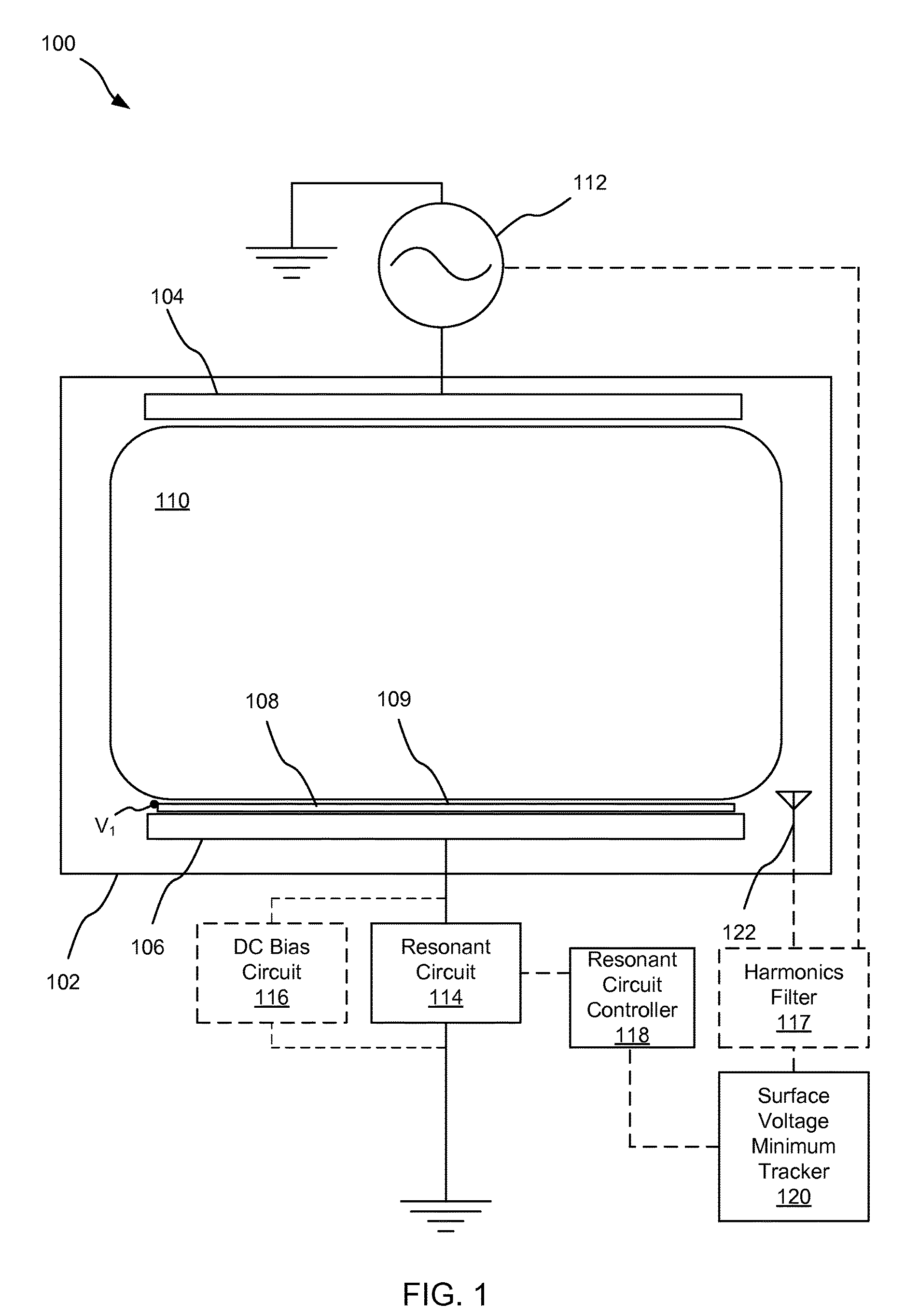
Figure 2 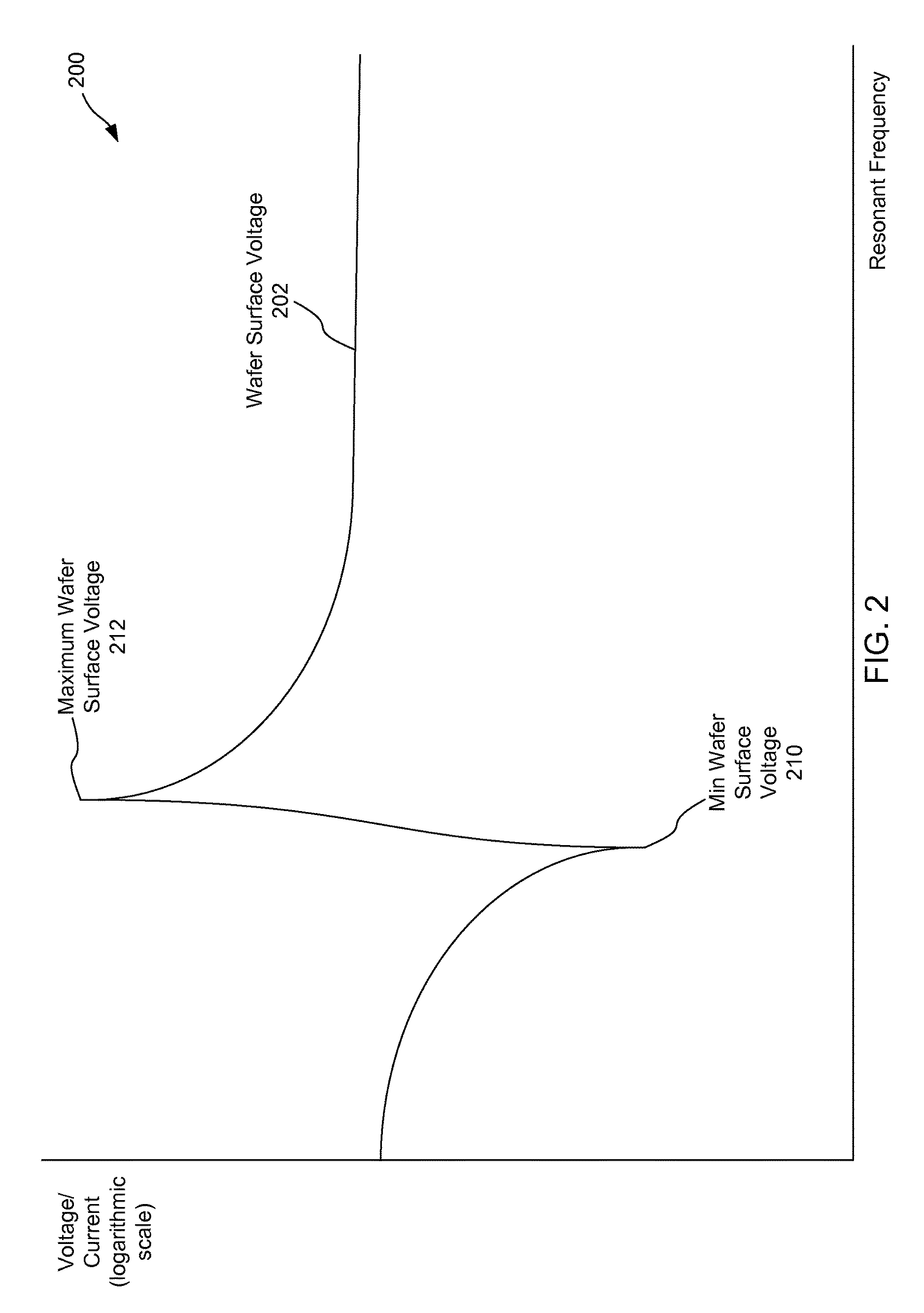
Figure 3
Abstract
Description
CLAIM OF PRIORITY UNDER 35 U.S.C. §119
[0001] The present Application for Patent claims priority to Provisional Application No. 61 / 856,485 entitled “SYSTEMS, METHODS, AND APPARATUS FOR MINIMIZING CROSS COUPLED WAFER SURFACE POTENTIALS” filed Jul. 19, 2013, and assigned to the assignee hereof and hereby expressly incorporated by reference herein.FIELD OF THE DISCLOSURE
[0002] The present disclosure relates generally to wafer processing. In particular, but not by way of limitation, the present disclosure relates to systems, methods and apparatuses for reducing a cross coupled potential on a wafer surface.BACKGROUND
[0003] Semiconductors are commonly formed in a plasma processing chamber where etching and deposition are enhanced by plasma generated ions that bombard the wafer substrate. The plasma can be ignited and sustained via radio frequency (RF) power from an RF source inductively or capacitively coupled into the plasma via application of the RF between a first electrode and a ground (e...
Examples
Embodiment Construction
[0021]In solving these challenges, the first realization that the inventors made was that, while a typical series LC resonant circuit has a single resonance (e.g., a single null), the series LC resonant circuit used in this context has two resonances, likely caused by stray capacitance and inductance. Modeling then indicated that the resonances were much closer to each other than expected.
[0022]FIG. 2 illustrates a wafer surface voltage plot based on such modeling. The wafer surface voltage 202 is plotted as a function of a capacitance in the series LC resonant circuit (or any other resonant circuit). The wafer surface voltage 202 has a minimum 210 at a given resonant circuit capacitance (or resonant frequency) and a maximum 212 at another resonant circuit capacitance (or resonant frequency). These resonances are so close to each other, that when existing systems were tuned for the minimum wafer surface voltage 210, slight variations in a resonant frequency of the resonant circuit w...