
Thin film transistor substrate for organic light-emitting diode display and manufacturing method thereof
a technology of light-emitting diodes and thin film transistors, which is applied in the direction of basic electric elements, electrical equipment, semiconductor devices, etc., can solve the problems of oxide semiconductor materials that are easily degraded by the light induced from the environment, uneven and/or rugged, etc., and achieves the reduction and/or minimization of contact holes, the effect of maximizing and optimizing the channel area of oxide semiconductor layers and ultra-high density
Patent Information
- Authority / Receiving Office
- US · United States
- Patent Type
- Patents(United States)
- Current Assignee / Owner
- Publication Date
- 2018-06-12
Smart Images
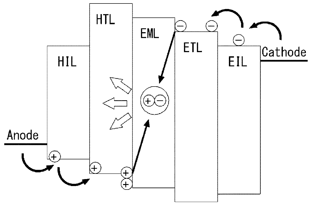
Figure 1 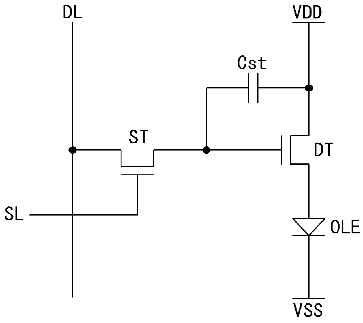
Figure 2 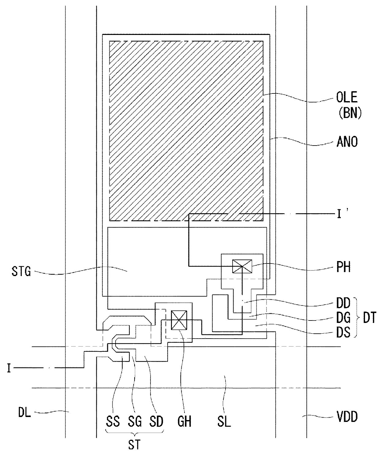
Figure 3
Abstract
Description
CROSS-REFERENCE TO RELATED APPLICATION(S)
[0001] This application claims the benefit of Korean Patent Application No. 10-2015-0166459, filed on Nov. 26, 2015, the entire disclosure of which is hereby incorporated by reference herein.BACKGROUND
[0002] 1. Technical Field
[0003] The present disclosure relates to a thin film transistor substrate for an organic light-emitting diode display having two different type thin film transistors on the same substrate, a display using the same, and a manufacturing method thereof.
[0004] 2. Discussion of the Related Art
[0005] Nowadays, as the information society develops, the requirements of displays for representing information are increasing. Accordingly, various flat panel displays (FPD) have been developed for overcoming many drawbacks of the cathode ray tube (CRT) display, which is heavy and bulky. The flat panel display devices include a liquid crystal display (LCD) device, a plasma display panel (PDP), an organic light-emitting diode (OLED) display d...
Examples
Embodiment Construction
[0037]Reference will now be made in detail to embodiments of the present disclosure, examples of which are illustrated in the accompanying drawings. In the following description, when a detailed description of well-known functions or configurations related to this document is determined to unnecessarily cloud a gist of the invention, the detailed description thereof will be omitted. The progression of processing steps and / or operations described is an example; however, the sequence of steps and / or operations is not limited to that set forth herein and may be changed as is known in the art, with the exception of steps and / or operations necessarily occurring in a certain order. Like reference numerals designate like elements throughout. Names of the respective elements used in the following explanations are selected only for convenience of writing the specification and may be thus different from those used in actual products.
[0038]In the description of embodiments, when a structure is...