Display device with capacitively connected pads
A display and display pixel technology, applied in static indicators, instruments, nonlinear optics, etc., can solve the problems of large matrix displays, hindering manufacturing, etc.
- Summary
- Abstract
- Description
- Claims
- Application Information
AI Technical Summary
Problems solved by technology
Method used
Image


Examples
Embodiment Construction
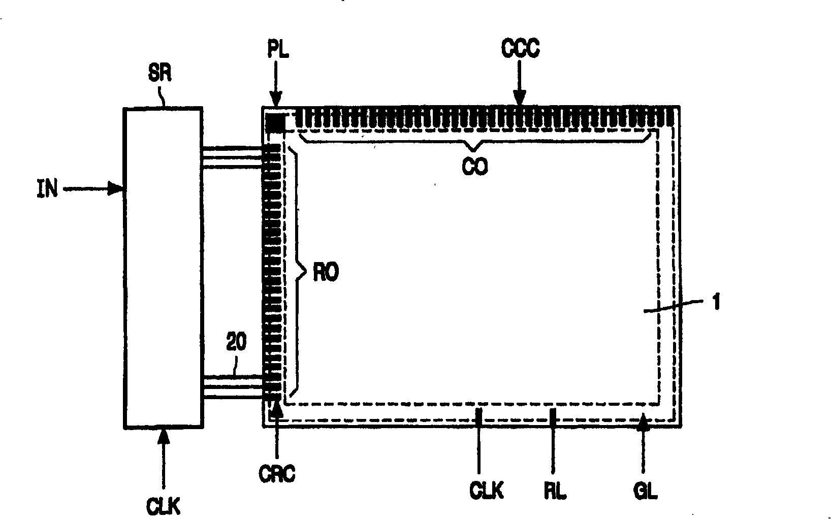
[0036] figure 1 A schematic diagram of a carrier and substrate with conductors for forming a capacitor is shown according to one embodiment of the invention.
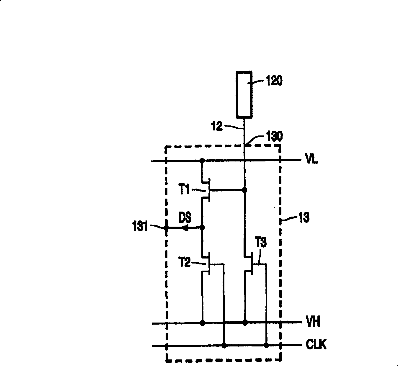
[0037] For simplicity, only one capacitor C is shown. If display 1 is with select electrode RO (see figure 2 ) and data electrodes CO, then multiple capacitors C are required, in principle at least one capacitor C is required for each select electrode RO and each data electrode CO. Also, capacitor C can be used to divide the clock signal CLK (see image 3 ), reference levels and / or power supplies (see Figure 4 ) to display 1.
[0038] The carrier 2 comprises a carrier conductor 20 which terminates in a pad 200 and carries an input signal IS. The display 1 comprises a substrate 16 and a display conductor 12 connected at one end to a display pixel 11 and terminated at the other end in a pad 120 . The display conductor 12 is located on the side of the substrate 16 facing away from the carrier conductor 20 so that t...
PUM
| Property | Measurement | Unit |
|---|---|---|
| thickness | aaaaa | aaaaa |
| thickness | aaaaa | aaaaa |
Abstract
Description
Claims
Application Information
 - R&D
- Intellectual Property
- Life Sciences
- Materials
- Tech Scout
- Unparalleled Data Quality
- Higher Quality Content
- 60% Fewer Hallucinations
Browse by: Latest US Patents, China's latest patents, Technical Efficacy Thesaurus, Application Domain, Technology Topic, Popular Technical Reports.
© 2025 PatSnap. All rights reserved.Legal|Privacy policy|Modern Slavery Act Transparency Statement|Sitemap|About US| Contact US: help@patsnap.com