Circuit board layout structure and method for preventing electromagnetic interference

A technology of electromagnetic interference and layout structure, applied in printed circuit parts, electrical components, magnetic field/electric field shielding, etc. It can solve the problems of complex electronic products and increase the manufacturing cost of electronic devices, so as to reduce the cost of electroplating and reduce the degree of noise radiation. , the effect of reducing the degree of mutual interference

Active Publication Date: 2009-07-01
UNIVERSAL SCIENTIFIC INDUSTRIAL (SHANGHAI) CO LTD
View PDF0 Cites 8 Cited by
  • Summary
  • Abstract
  • Description
  • Claims
  • Application Information

AI Technical Summary

Problems solved by technology

These electromagnetic wave prevention steps will increase the manufacturing cost of electronic devices and make electronic products more complex

Method used


Image

  • Circuit board layout structure and method for preventing electromagnetic interference
  • Circuit board layout structure and method for preventing electromagnetic interference
  • Circuit board layout structure and method for preventing electromagnetic interference

Examples


Embodiment Construction

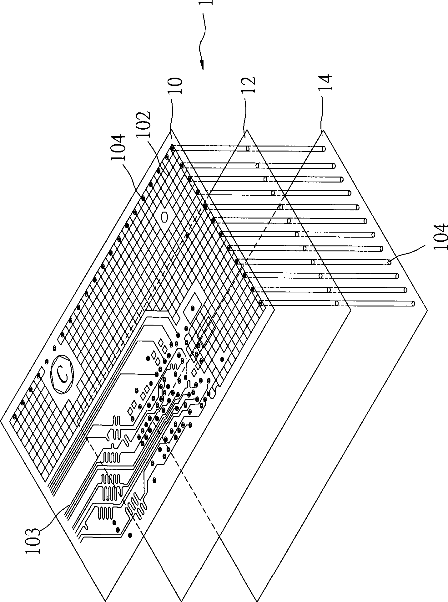
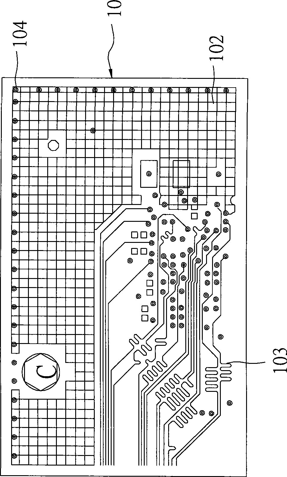
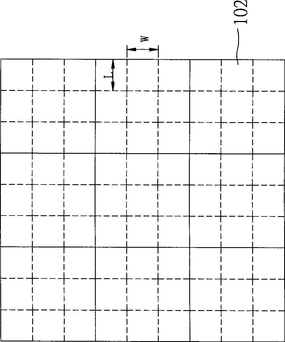
[0030] Please refer to figure 1 , which is a layered schematic diagram of the circuit board layout structure of the present invention. Wherein, the circuit board layout structure of the present invention includes a multilayer printed circuit board 1 , a plurality of conductive grids 102 and a plurality of conductive through holes 104 . The multilayer printed circuit board 1 has a first signal layer 10 , a second signal layer 14 and a ground layer 12 . A plurality of signal lines 103 and a plurality of conductive grids 102 are arranged on the first signal layer 10 and the second signal layer 14 , wherein the plurality of conductive grids 102 are used to cover the aforementioned plurality of signal lines 103 . Meanwhile, the plurality of conductive vias 104 are electrically connected to the ground layer 12 and electrically connected to the plurality of conductive grids 102 on the first signal layer 10 and the second signal layer 14 .

[0031] Cooperate figure 1 , please refer...


PUM


Abstract

The invention relates to a circuit board layout structure and a method for preventing electromagnetic interference, wherein, the circuit board layout structure comprises a multilayer printed circuit board, a plurality of conduction grids and a plurality of conduction perforations. The multilayer printed circuit board is provided with a plurality of signal layers and a grounding layer; a plurality of signal circuits are arranged on each signal layer; the conduction grids wrapping the signal circuits on each signal layer are distributed on each signal layer; and the conduction perforations are formed among the layers of the multilayer printed circuit board, and electrically connected to the grounding layer and conduction grids on each signal layer. Therefore, according to the design of the size of the conduction grids, the purpose of blocking the frequency of a specialized electromagnetic wave can be achieved. The invention can reduce the length distributed by a field of interference sources, so as to weaken noise radiation degree, further reduce the mutual interference degree of signals, reduce the number of the conduction perforations by about 30 to 50 percent, and avoid the intensity reduction of the circuit board. In addition, the invention adopts a mode of conduction grid layout, thereby reducing the electroplating cost by about 25 to 30 percent.

Description

technical field [0001] The invention relates to a circuit board layout structure and method for preventing electromagnetic interference, in particular to a circuit board layout structure and method for preventing electromagnetic interference with high-frequency signals. Background technique [0002] Any high-frequency electronic product will generate noise (Noise). Electronic noise interference can be divided into two aspects: conducted interference and radiated interference. Generally speaking, conducted interference will interfere with the power line to affect the normal operation of other electronic or electrical products. , and radiated interference is to interfere with other equipment through the air. For the use of electrical appliances, the general national electrical safety regulations have formulated regulations to prevent electromagnetic interference. [0003] With the advancement of high-tech fields, the problems of electromagnetic interference (EMI) are also incr...

Claims


Application Information

Patent Timeline
Patent Type & Authority Applications(China)
IPC IPC(8): H05K9/00H05K1/02
Inventor 叶洧豪洪颖福
Owner UNIVERSAL SCIENTIFIC INDUSTRIAL (SHANGHAI) CO LTD
Why Eureka
Try Eureka