Semiconductor packaging structure

A semiconductor and structure technology, applied in the field of uniform conduction semiconductor packaging structure, can solve problems such as high cost and uneven heat dissipation of indium sheets

Inactive Publication Date: 2013-01-16
ADVANCED SEMICON ENG INC
View PDF5 Cites 14 Cited by
  • Summary
  • Abstract
  • Description
  • Claims
  • Application Information

AI Technical Summary

Problems solved by technology

[0006] In view of this, the present invention provides a semiconductor packaging structure to solve the problems of uneven heat dissipation and high cost in existing semiconductor packaging structures using indium sheets for heat dissipation

Method used


Image

  • Semiconductor packaging structure
  • Semiconductor packaging structure
  • Semiconductor packaging structure

Examples


Embodiment Construction

[0016] The following descriptions of the various embodiments refer to the accompanying drawings to illustrate specific embodiments in which the present invention can be practiced. Furthermore, the directional terms mentioned in the present invention, such as "upper", "lower", "top", "bottom", "front", "back", "left", "right", "inside", " Outer, Side, Surround, Center, Horizontal, Horizontal, Vertical, Longitudinal, Axial, Radial, Topmost, or Bottommost etc. are merely for reference to the directions of the attached drawings. Therefore, the directional terms used are used to illustrate and understand the present invention, but not to limit the present invention.

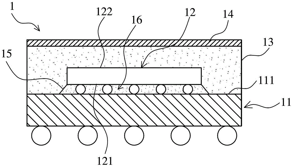
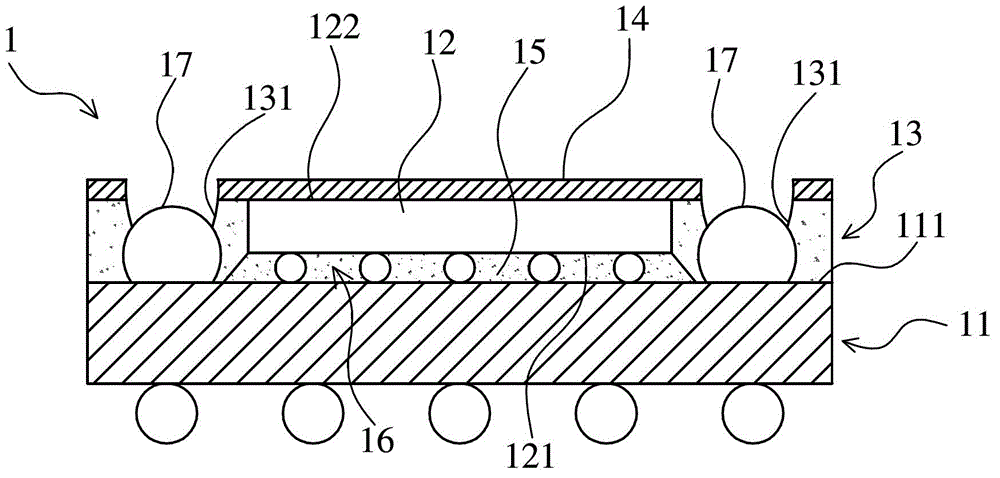
[0017] Please refer to figure 1 As shown, it discloses the semiconductor package structure of the first embodiment of the present invention. Hereinafter, the semiconductor package structure is directly referred to as a package body 1 . In this embodiment, the package 1 includes: a substrate 11 , a chip 12 , an enca...


PUM


Abstract

The invention discloses a semiconductor packaging structure which comprises a substrate, at least one chip, a packaging colloid and a grapheme layer. The grapheme layer is arranged on the packaging colloid or arranged on the surface e of the chip. By means of the grapheme layer, the semiconductor packaging structure has high planarity heat-conductivity coefficient, facilities lateral heat conductivity, increases even conduction of heat and heat exchange area, and further improves the heat conducting-out efficiency of the chip.

Description

technical field [0001] The present invention relates to a semiconductor packaging structure, in particular to a semiconductor packaging structure that increases the uniform conduction of heat. Background technique [0002] Nowadays, with the miniaturization, multi-function and high-performance of electronic devices such as portable personal computers, smart phones and digital cameras, semiconductor devices must be designed to be smaller and have more functions, thus making semiconductor package structure (semiconductor package) ) are becoming more and more common in the use of many electronic devices. However, the chip tends to generate high temperature during operation, so a heat sink needs to be bonded to the surface of the chip to improve the overall heat dissipation efficiency. A common way to fix the heat sink on the chip is to use thermally conductive adhesive, but it is not easy to control the thickness uniformity of the thermally conductive adhesive when bonding, an...

Claims


Application Information

Patent Timeline
Patent Type & Authority Applications(China)
IPC IPC(8): H01L23/373H01L23/31
CPCH01L2224/16227H01L2224/32225H01L2224/73204H01L2225/1023H01L2225/1058H01L2225/1094H01L2924/15311H01L2924/15331H01L2924/1815H01L2224/16225H01L2924/00
Inventor 洪志斌翁肇甫谢慧英
Owner ADVANCED SEMICON ENG INC
Why Eureka
Try Eureka