
Improved method of bipolar integrated circuit amplification coefficient process
An integrated circuit and process improvement technology, which is applied in the field of semiconductor manufacturing technology, can solve the problems of bipolar circuit amplification factor attenuation, stress characteristic circuit incomplete matching, etc., and achieve the effect of stabilizing the PNP tube amplification factor, preventing attenuation, and being easy to implement
- Summary
- Abstract
- Description
- Claims
- Application Information
AI Technical Summary
Problems solved by technology
Method used
Image

Examples
Embodiment Construction
[0022] The method for improving the amplification factor process of a bipolar integrated circuit provided by the present invention includes the steps of manufacturing the basic circuit of a bipolar integrated circuit compatible with BJT and JFET by conventional technology, the step of manufacturing electrode leads on the basic circuit, and the subsequent process finishing step .
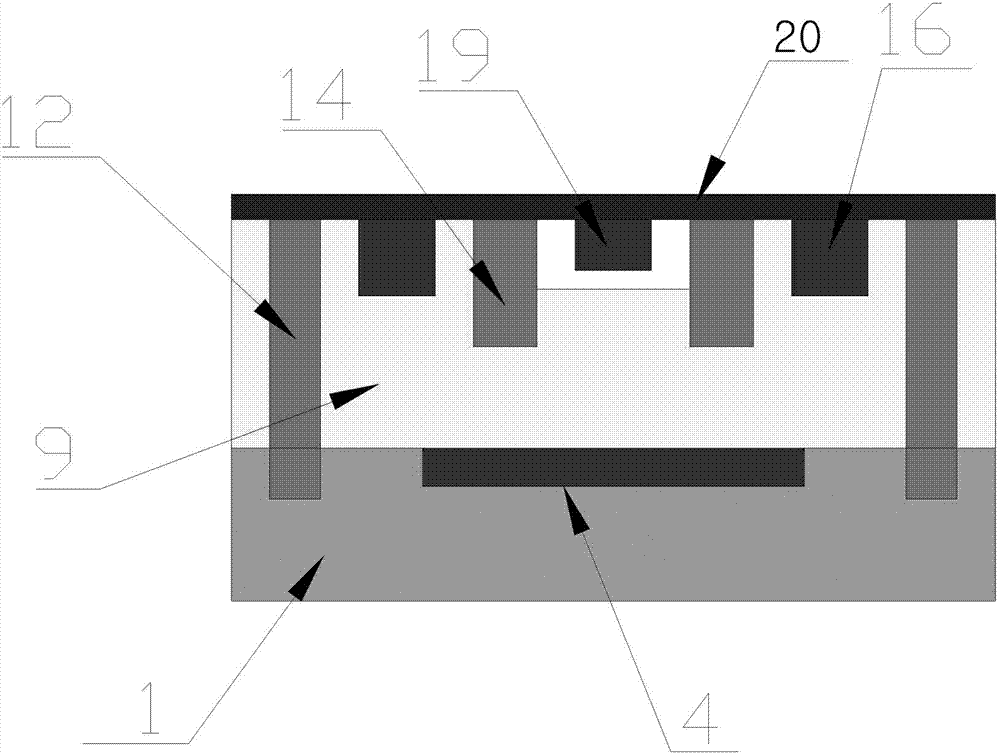
[0023] The basic circuit includes the underlying silicon P substrate 1, N - Epitaxial layer 9, P+ region 12, N+ region 4, base region boron (14), emitter region phosphorus (16) and gate region phosphorus (19).
[0024] The present invention is characterized in that the step of making electrode leads on the described basic circuit is:
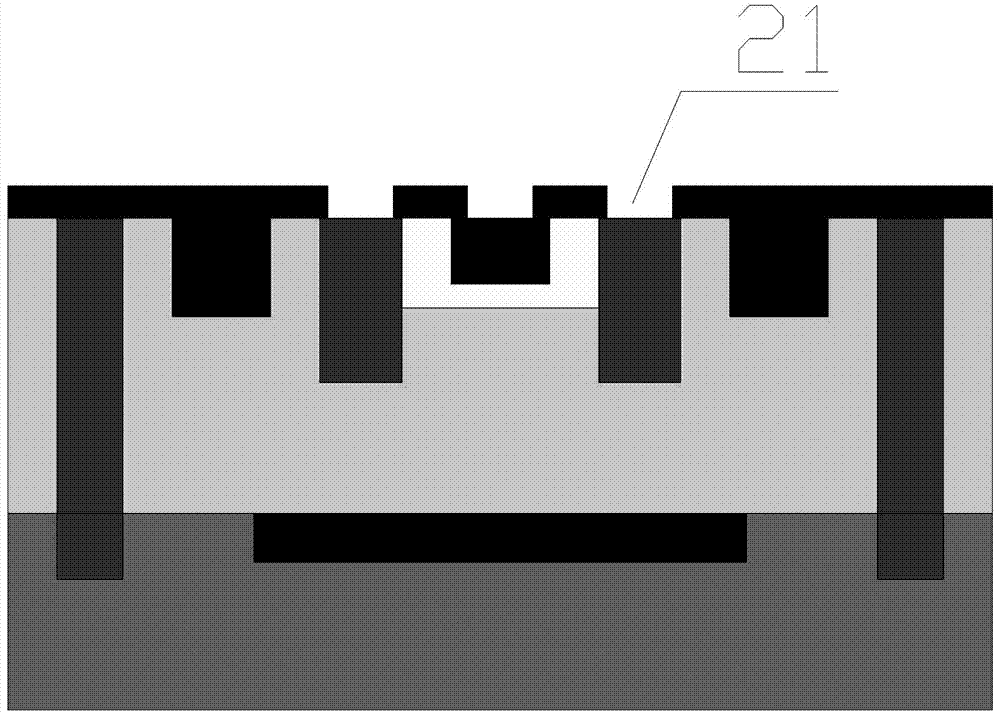
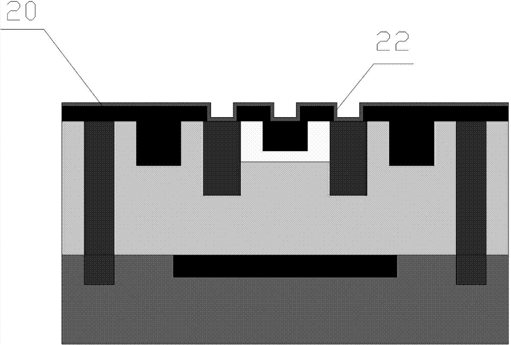
[0025] a. Depositing LTO - such as figure 1 As shown, at a furnace temperature of 420 ° C, a layer of silicon dioxide 20 of about 450 nm is deposited by LPCVD (vapor phase deposition device) as a circuit capacitor dielectric layer; then the deposited LTO layer is pro...
PUM
 Abstract
Description
Claims
Application Information