Wiring structure

A wiring structure and wiring technology, applied in nonlinear optics, instruments, optics, etc., can solve the problems that single-layer metal wiring cannot reduce the wiring area, affect the display quality, and cannot achieve the narrow-edge design of the liquid crystal panel. To achieve the effect of solving the display quality

Active Publication Date: 2013-10-02
NANJING CEC PANDA LCD TECH
View PDF9 Cites 13 Cited by
  • Summary
  • Abstract
  • Description
  • Claims
  • Application Information

AI Technical Summary

Problems solved by technology

[0005] Purpose of the invention: to solve the problems in the prior art that the single-layer metal wiring cannot narrow the wiring area and cannot achieve the narrow-edge design of the liquid crystal panel, and the problem that the signal interference between the two wiring layers affects the display quality

Method used


Image

  • Wiring structure
  • Wiring structure
  • Wiring structure

Examples


Embodiment Construction

[0023] Below in conjunction with accompanying drawing and specific embodiment, further illustrate the present invention, it should be understood that these embodiments are only used to illustrate the present invention and are not intended to limit the scope of the present invention, after having read the present invention, those skilled in the art understand various aspects of the present invention Modifications in equivalent forms all fall within the scope defined by the appended claims of this application.

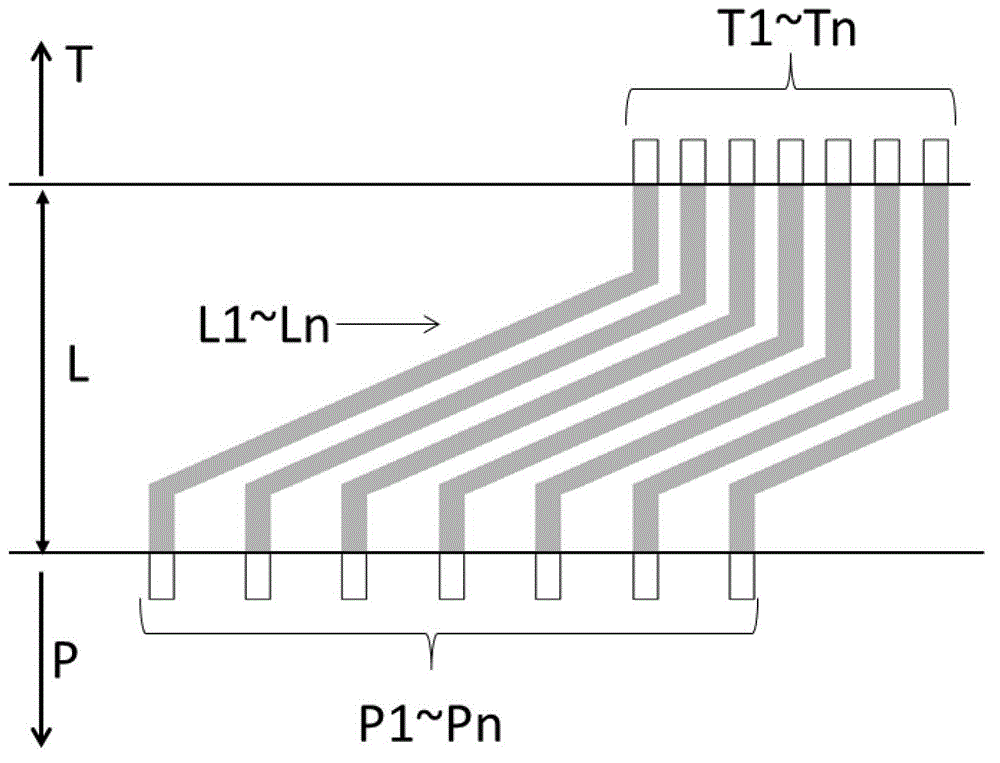
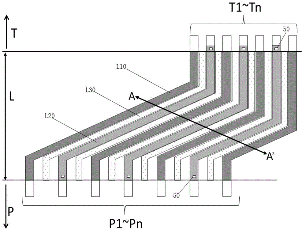
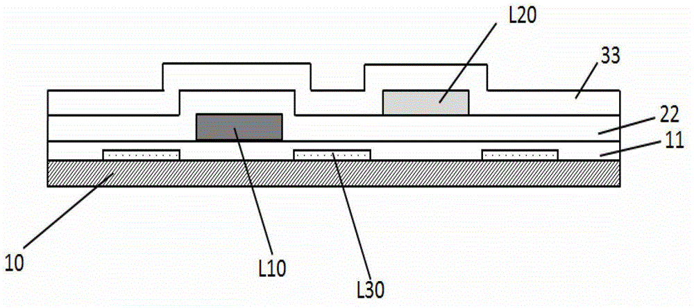
[0024] In order to reduce the wiring area to achieve the narrow design of the liquid crystal display, the present invention provides a wiring structure of a TFT-LCD array substrate, such as figure 2 Shown is a partial schematic diagram of the wiring structure of the present invention. The surface of the TFT-LCD array substrate has a pixel area P (that is, the display area), which is defined by the intersection of multiple scanning lines and multiple data signal lines; a...


PUM


Abstract

The invention discloses a wiring structure, which is applied to TFT-LCD (thin film transistor liquid crystal display) array substrate, wherein the substrate has a pixel region, a wiring region, a terminal region and a TFT array; the pixel region is limited crossly by a plurality of scanning lines and a plurality of data signal lines; the wiring region and the terminal region are arranged on the outer side of the pixel region; the TFT array is formed on the substrate and is arranged in the pixel region; the wiring region comprises a plurality of first wires formed by first wiring layers and a plurality of second wires formed by second wiring layers; the first wires and the second wires are alternatively configured, and a shielding electrode is arranged between each first wire and each second wire; the first wires and the second wires electrically connect a plurality of pixel terminals with a plurality of signal terminals. Through the scheme of the invention, the problem of wire width and wire distance easily generated in a single-layer metal wire is solved through the double-layer wire; meanwhile, an ITO (indium tin oxide) transparent electrode arranged between the two adjacent wires is used for isolating signal interference, so that the problem that the display quality is influenced by the signal interference between the two layers of wires is solved.

Description

technical field [0001] The invention relates to a wiring structure, in particular to a double-layer wiring structure of a TFT-LCD array substrate. Background technique [0002] With the development of the Thin Film Transistor Liquid Crystal Display (TFT-LCD) industry and the growing demands of consumers, thinner and thinner LCD displays with beautiful appearance and sharp sharpness have become a popular trend. At the same time, the reduction of ICs for LCDs and the design requirements of Fine Pith COF (Chip on Film) \ COG (Chip on Glass) are also increasing the requirements for narrow frontal margins of LCDs. [0003] The main factor affecting the determination of the narrow frame is the wiring area of ​​the TFT-LCD array substrate of the liquid crystal display, such as figure 1 Shown is a partial schematic diagram of a liquid crystal display TFT-LCD array substrate in the prior art. The surface of the substrate 100 has a pixel area P (ie, a display area), a wiring area L a...

Claims


Application Information

Patent Timeline
Patent Type & Authority Applications(China)
IPC IPC(8): G02F1/1362G02F1/1368G02F1/1343
Inventor 周刘飞何建国
Owner NANJING CEC PANDA LCD TECH
Why Eureka
Try Eureka