Array substrate, display panel and display device

A technology for array substrates and display panels, which is applied in the fields of array substrates, display panels and display devices, and can solve problems such as breakdown of display panel integrated circuits and damage to display panel integrated circuits

Active Publication Date: 2014-04-02
BOE TECH GRP CO LTD +1
View PDF4 Cites 18 Cited by
  • Summary
  • Abstract
  • Description
  • Claims
  • Application Information

AI Technical Summary

Problems solved by technology

[0006] Embodiments of the present invention provide an array substrate, a display panel, and a display device, which are used to solve the problem that when the existing display panel is squeezed or rubbed, a large

Method used


Image

  • Array substrate, display panel and display device
  • Array substrate, display panel and display device
  • Array substrate, display panel and display device

Examples


Embodiment Construction

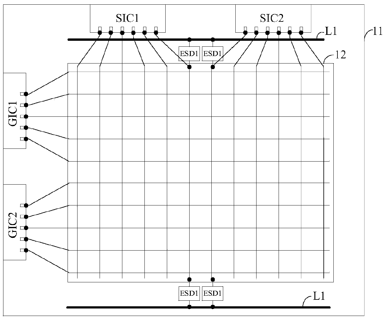
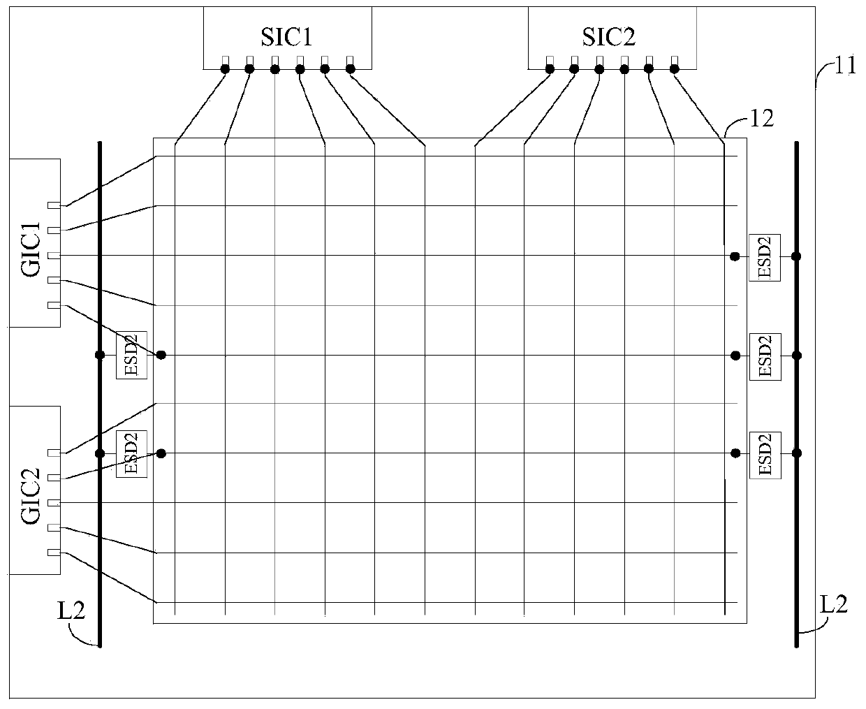
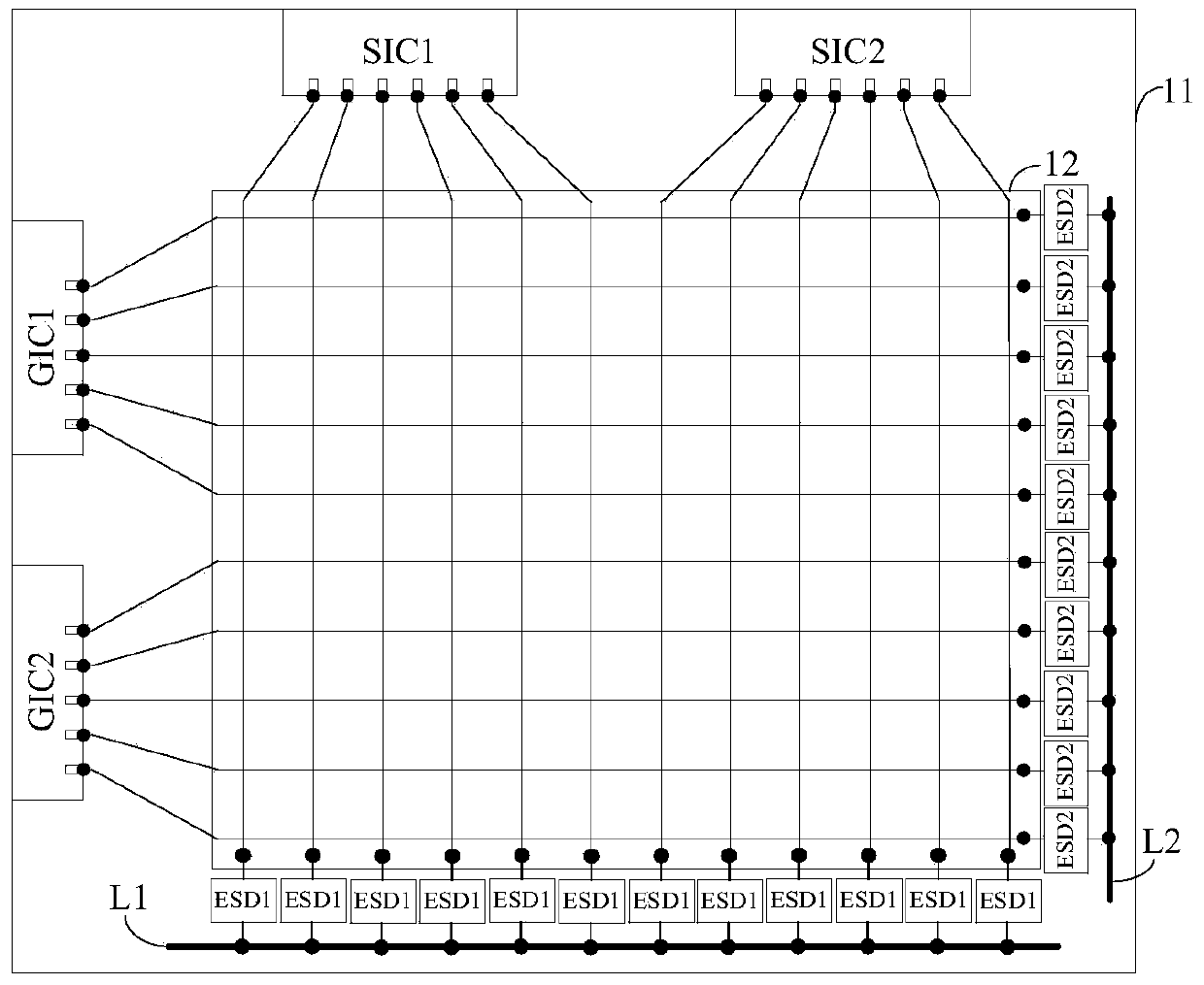
[0020] An embodiment of the present invention provides an array substrate, in which at least one data line is connected to a first lead on the array substrate through at least one first electrostatic discharge device, and each first electrostatic discharge device is only connected to one data line. line, in the display panel including the array substrate, the integrated circuit connected to the data line connected to the first electrostatic discharge device accumulates charge, and the accumulated charge can make the first electrostatic discharge device connected to the data line turn on, the connection The charge accumulated in the integrated circuit of the data line can be released to the first lead through the first electrostatic discharge device, thereby preventing the accumulated charge from breaking down the integrated circuit; and the charge accumulated in the integrated circuit connected to the data line is discharged When the first electrostatic discharge device connect...


PUM


Abstract

An embodiment of the invention provides an array substrate, a display panel and a display device, aiming to solve the problem that when the existing display panel is squeezed or rubbed, a great quantity of electric charges can be accumulated in integrated circuits thereof to be even possible to break down the same, thereby resulting damages to the integrated circuits in the display panel. The array substrate comprises multiple data lines and multiple gate lines; at least one data line is connected with a first lead on the array substrate through at least one first electrostatic discharger, each first electrostatic discharger is connected with one data line only; or at least one gate line is connected to a second lead on the array substrate through at least one second electrostatic discharger, and each second electrostatic discharger is connected one gate line only.

Description

technical field [0001] The present invention relates to the field of display technology, in particular to an array substrate, a display panel and a display device. Background technique [0002] Existing display devices can use a variety of different display panels, for example, organic light-emitting diode (OLED, Organic Light-Emitting Diode) panels, thin film transistor liquid crystal displays (TFT-LCD, Thin Film Transistor Liquid Crystal Display). The following uses TFT-LCD as an example to illustrate the important component of the display panel - the array substrate. [0003] The existing TFT-LCD is formed by combining an array substrate and a color filter substrate. On the array substrate, gate lines and data lines defining pixel areas are arranged to cross each other, and pixel electrodes and thin film transistors are arranged in each pixel area. Driving signals are applied to the gate lines, and image data is applied to the pixel electrodes through the signal lines. ...

Claims


Application Information

Patent Timeline
IPC IPC(8): G02F1/1362H01L27/02
CPCH01L27/0296G02F1/136204G09G3/3611G09G2330/04G09G3/20G09G2330/025G09G2330/06G02F1/133388G09G3/006G09G3/2092G09G2330/08
Inventor 闫岩
Owner BOE TECH GRP CO LTD
Why Eureka
Try Eureka