

Reaction chamber and plasma processing equipment
A reaction chamber and plasma technology, applied in the direction of plasma, metal material coating process, gaseous chemical plating, etc., can solve the problems of process influence and process stability, etc. Effect
- Summary
- Abstract
- Description
- Claims
- Application Information
AI Technical Summary
Problems solved by technology
Method used
Image

Examples
Embodiment Construction
[0029] In order for those skilled in the art to better understand the technical solution of the present invention, the reaction chamber and the plasma processing equipment provided by the present invention will be described in detail below with reference to the accompanying drawings.
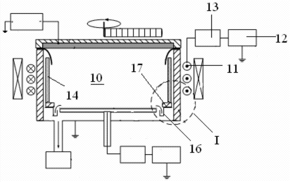
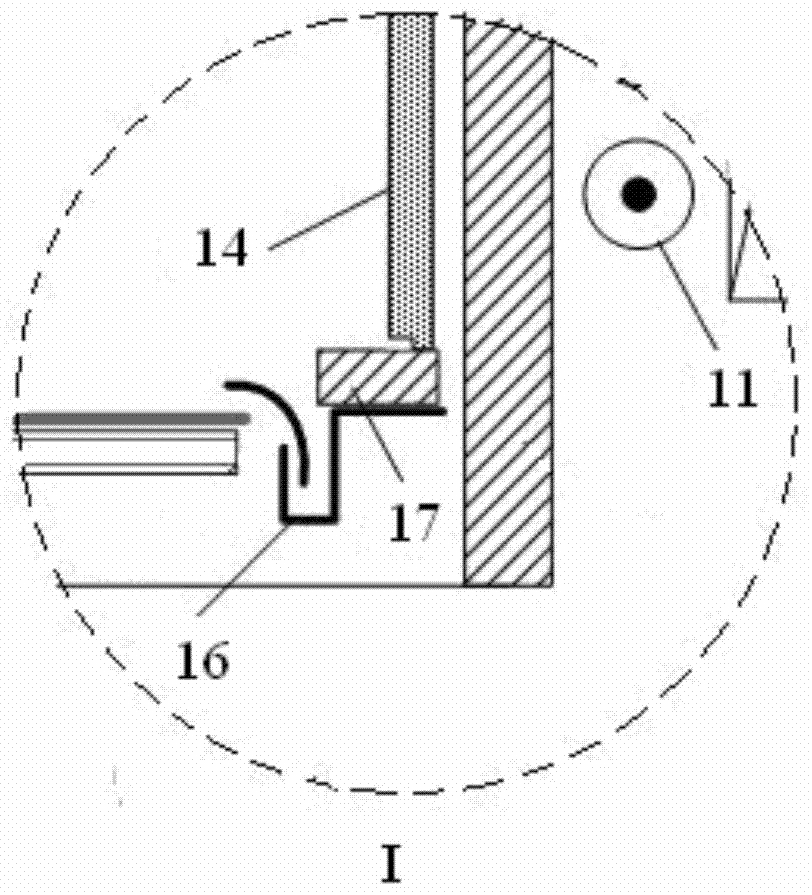
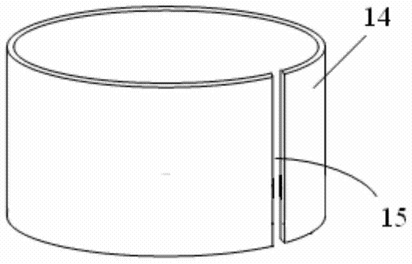
[0030] Figure 4 Schematic diagram of the structure of the reaction chamber provided by the first embodiment of the present invention. Figure 5 for Figure 4 Schematic diagram of the structure of the Faraday shield, insulating ring and shielding ring in the middle. Please also refer to Figure 4 with Figure 5 The reaction chamber 20 provided in this embodiment includes a Faraday shield 21 sleeved inside the side wall of the reaction chamber 20, an insulating ring 22, a shielding ring 23 made of a non-magnetic metal material, an induction coil 24 and A radio frequency power supply 25 electrically connected thereto. Wherein, the Faraday shield 21 is stacked on the insulating ring 22, at lea...
PUM
 Abstract
Description
Claims
Application Information