Method for preventing transverse diffusion of ohmic contact aluminum in GaN-based device

A technology of ohmic contact and aluminum elements, applied in semiconductor devices, semiconductor/solid-state device manufacturing, electrical components, etc., can solve problems such as the lateral diffusion of aluminum elements, reduce interface states, reduce interface pollution, and avoid the risk of deteriorating device performance Effect

CN105206524AInactive Publication Date: 2015-12-30INST OF MICROELECTRONICS CHINESE ACAD OF SCI
5 Cites 1 Cited by

Patent Information

Authority / Receiving Office
CN · China
Patent Type
Applications(China)
Current Assignee / Owner
Publication Date
2015-12-30
Estimated Expiration
Not applicable · inactive patent

Smart Images

  • Figure 1
    Figure 1
  • Figure 2
    Figure 2
Patent Text Reader

Abstract

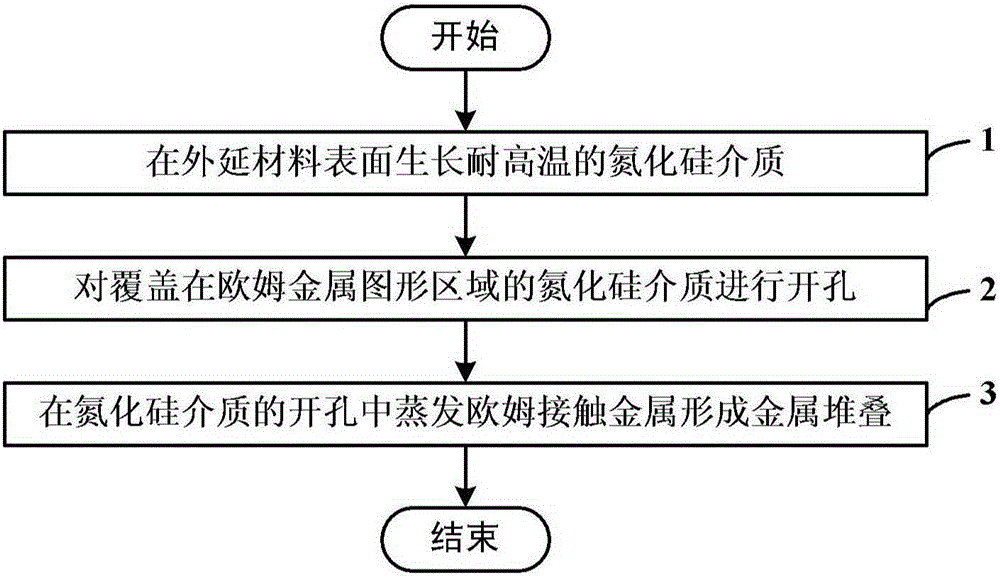
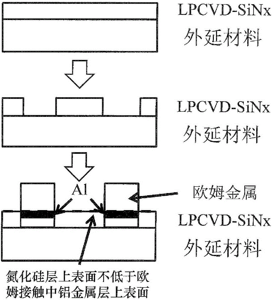
The invention discloses a method for preventing transverse diffusion of ohmic contact aluminum in a GaN-based device. Ohmic contact aluminum is deposited in pores of a heat-resisting silicon nitride medium, transverse diffusion of ohmic contact aluminum is blocked by the heat-resisting silicon nitride medium, surface protection for ohmic alloy is further realized, and interface pollution and interface state are reduced. The method comprises: the heat-resisting silicon nitride medium grows on the surface of an epitaxial material; pores are formed in the high-temperature silicon nitride medium covering the area of an ohmic contact metal pattern; ohmic contact metal is evaporated in the formed pores of the silicon nitride medium to form metal stacking, wherein the upper surface of the silicon nitride medium is not lower than the upper surface of a stacked metal aluminum layer in the area of the formed pores. The method solves the problem of aluminum transverse diffusion in ohmic contact preparation of the GaN-based device, avoids the risk that the device performance is degraded due to a polluted material surface in a high-temperature alloy technology, further realizes surface protection of ohmic alloy, and reduces interface pollution and interface state.
Need to check novelty before this filing date? Find Prior Art

Description

technical field

[0001] The invention relates to the technical field of ohmic contact and passivation technology in GaN-based devices, in particular to a method for preventing lateral diffusion of aluminum elements in ohmic contacts in GaN-based devices. Background technique

[0002] The ohmic contact metal system of mainstream GaN-based devices usually contains an aluminum metal layer. The purpose of introducing the aluminum metal layer is to reduce the resistivity of the ohmic contact. However, the latest research has found that aluminum is easy to diffuse laterally in high-temperature alloys, and oxidizes and deposits at high temperatures. On the surface of the epitaxial material, the surface state of the epitaxial material remains high, reducing device performance.

[0003] In addition, considering the ultra-high temperature conditions of the alloy greater than 800°C, the silicon nitride dielectric grown at low temperature has a large thermal mismatch with the gallium nit...

Examples

Embodiment Construction

[0017] In order to make the object, technical solution and advantages of the present invention clearer, the present invention will be described in further detail below in conjunction with specific embodiments and with reference to the accompanying drawings.

[0018] Such as figure 1 as shown, figure 1 It is a flow chart of the method for preventing lateral diffusion of ohmic-contact aluminum elements in GaN-based devices provided by the present invention. The method is to deposit ohmic-contact aluminum elements in high-temperature-resistant silicon nitride dielectric holes, and block ohmic contacts through silicon nitride dielectrics. The lateral diffusion of aluminum elements, and then realize the surface protection of ohmic alloys, reduce interface pollution and interface states. The method specifically includes the following steps:

[0019] Step a: growing a high temperature resistant silicon nitride dielectric on the surface of the epitaxial material;

[0020] In this st...