Array substrate, display panel and display device

An array substrate and display panel technology, applied in semiconductor devices, electrical components, photovoltaic power generation, etc., can solve the problems of easy ghosting, affecting the visual effect of the display screen, and the display screen is not clear, and achieves the effect of realizing a borderless design.

Active Publication Date: 2018-10-12
BOE OPTICAL SCI & TECH +1
View PDF6 Cites 0 Cited by
  • Summary
  • Abstract
  • Description
  • Claims
  • Application Information

AI Technical Summary

Problems solved by technology

The display panel includes a display area and a peripheral area, wherein the peripheral area includes a chip for controlling the pixel units in the display area. Since the chip occupies the peripheral area of ​​the display panel, the peripheral area of ​​the display panel will be set wider, so that the display panel The frame area occupies a large area, which affects the visual effect of the display screen
[0003] At present, in order to realize the borderless display effect of the display panel, there are the following two methods: one is to make the size of the display module the same as the size of the glass cover, cancel the border of the display panel, and it looks It is borderless, but users will still see the black border around the screen when they actually watch it; another method is to set optical components on the edge of the glass cover to guide light into the border area on the edge of the panel, so that users can watch It results in a visual borderless display effect, but the brightness of the border area of ​​the display panel produced in this way is darker than that of the normal display area, the display picture is not clear, and ghosting is prone to occur, resulting in poor display effect

Method used


Image

  • Array substrate, display panel and display device
  • Array substrate, display panel and display device
  • Array substrate, display panel and display device

Examples


Embodiment Construction

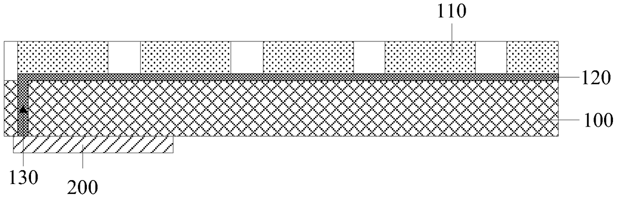
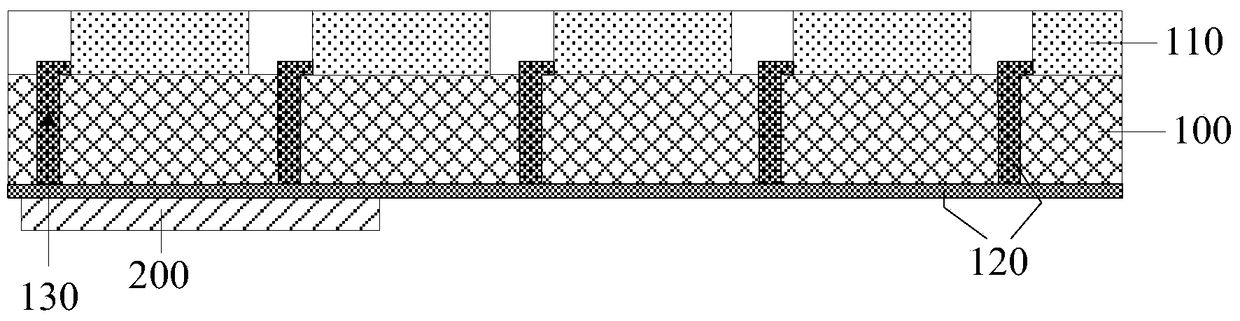
[0031] The specific implementation manners of the array substrate, the display panel and the display device provided by the embodiments of the present invention will be described in detail below with reference to the accompanying drawings.

[0032] The thickness and shape of each film layer in the drawings do not reflect the real scale, and the purpose is only to illustrate the content of the present invention.

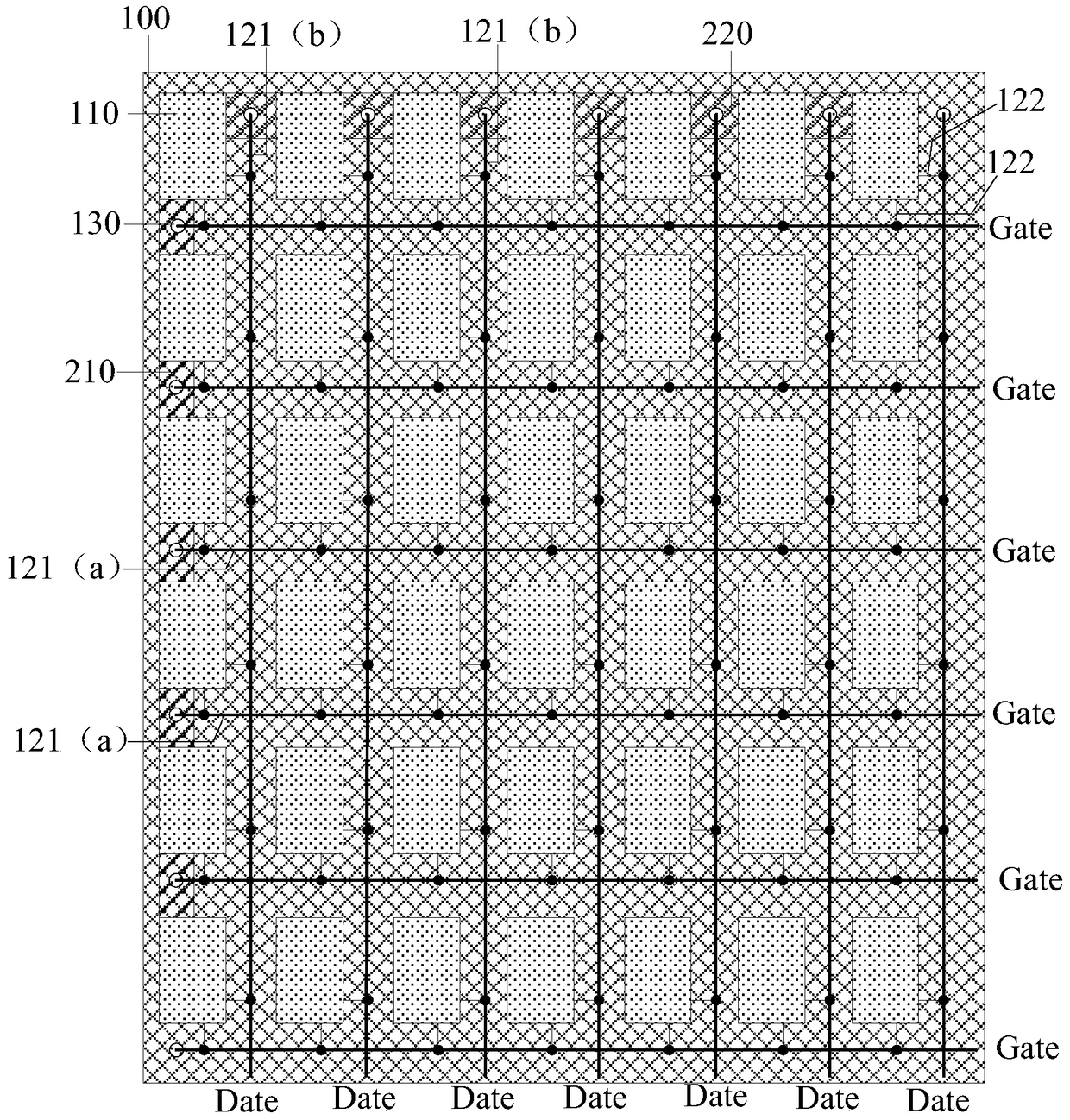
[0033] An embodiment of the present invention provides an array substrate, such as Figure 1a and Figure 1b As shown, it includes: a base substrate 100, a plurality of pixel units 110 arranged in a matrix on one side of the base substrate 100, a chip 200 for providing signals to each pixel unit 110, and a signal corresponding to each pixel unit 110 line 120, the chip 200 is located on the opposite side of the base substrate 100 where the pixel unit 110 is disposed; the array substrate is also provided with a via hole 130 at least penetrating the base substrate 100; t...


PUM


Abstract

The invention discloses an array substrate, a display panel and a display device, comprising: a base substrate, a plurality of pixel units arranged in a matrix on one side of the base substrate, a chip for providing signals to each pixel unit, and each pixel The signal line corresponding to the unit, and the via hole passing through the substrate; by setting the chip on the opposite side of the substrate where the pixel unit is provided, the signal line electrically connects the pixel unit to the chip through the via hole, thereby saving The frame part used to place the chip in the prior art is removed, thereby realizing a real frameless design.

Description

technical field [0001] The present invention relates to the field of display technology, in particular to an array substrate, a display panel and a display device. Background technique [0002] With the continuous development of display technology, display panels for mobile terminals such as personal computers, portable terminals, and various information equipment are developing rapidly. Most of the mobile terminals on the market use liquid crystal display devices, plasma display devices, and field emission display devices. , organic light emitting diode display devices and other flat panel display devices as the display panel. The display panel includes a display area and a peripheral area, wherein the peripheral area includes a chip for controlling the pixel units in the display area. Since the chip occupies the peripheral area of ​​the display panel, the peripheral area of ​​the display panel will be set wider, so that the display panel The frame area of ​​the frame occu...

Claims


Application Information

Patent Timeline
Patent Type & Authority Patents(China)
IPC IPC(8): H01L27/12H01L27/32
CPCH01L27/12Y02E10/549H10K59/131H10K77/10H01L29/78669H01L27/1248H10K59/1275
Inventor 王涛
Owner BOE OPTICAL SCI & TECH
Why Eureka
Try Eureka