Manufacturing method of display panel, display panel and display device

A technology of a display panel and a manufacturing method, which is applied in the direction of semiconductor devices, electrical components, circuits, etc., can solve the problems of consumers' simplicity and contradiction, and achieve the effect of realizing a borderless design.

Active Publication Date: 2021-01-22
BOE TECH GRP CO LTD
View PDF8 Cites 0 Cited by
  • Summary
  • Abstract
  • Description
  • Claims
  • Application Information

AI Technical Summary

Problems solved by technology

[0003] Today, consumers are pursuing simplicity in the appearance of display panels, but due to the composition of the display panel structure, as well as its overall strength requirements, reliability requirements, optical architecture and other factors, the display panel needs a frame to cover the flip-chip on the substrate. Thin film layer, which is contrary to the simplicity sought by consumers

Method used


Image

  • Manufacturing method of display panel, display panel and display device
  • Manufacturing method of display panel, display panel and display device

Examples


Embodiment 1

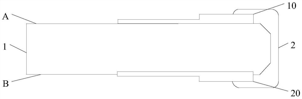
[0025] Embodiment 1 of the present invention provides a method for manufacturing a display panel, including: a substrate 1, the substrate 1 has a first surface A and a second surface B opposite to the first surface A, refer to figure 1 As shown, its production method may include:

[0026] depositing an array layer 10 on the first surface A;

[0027] depositing a chip-on-film layer 20 on the second surface B;

[0028] A connection line 2 is provided on the side surface of the substrate 1 , and two ends of the connection line 2 are respectively connected to the array layer 10 and the chip-on-film layer 20 .

[0029] Specifically, the substrate 1 can be made of a high-temperature resistant material to ensure that the substrate 1 can withstand high-temperature baking during high-temperature annealing when the array layer 10 is deposited; the connecting wire 2 can be a metal wire, such as a wire made of silver material; the connecting wire 2 It can be attached to the side surface...

Embodiment 2

[0088] Based on the same inventive concept, the second embodiment of the present invention provides a display panel, which is manufactured according to the above manufacturing method, refer to figure 1 shown, the display panel includes:

[0089] The substrate 1 has a first surface A and a second surface B opposite to the first surface A, the first surface A is provided with an array layer 10, and the second surface B is provided with a chip-on-film layer 20;

[0090] The connection line 2 is disposed on the side surface of the substrate 1 , and two ends of the connection line 2 are electrically connected to the array layer 10 and the chip-on-film layer 20 respectively.

[0091] Specifically, by disposing the array layer 10 on the first surface A of the substrate 1, and disposing the chip-on-film layer 20 on the second surface B of the substrate 1, the first surface A and the second surface B are opposite to each other. At the same time, the side surface of the substrate 1 is ...

Embodiment 3

[0097] Based on the same inventive concept, Embodiment 3 of the present invention provides a display device, which includes: the above-mentioned display panel.

[0098] Specifically, the display device may be any product or component with a display function, such as a tablet computer, a television, electronic paper, a mobile phone, a monitor, a notebook computer, a digital photo frame, and a navigator.

[0099] The display device provided in this embodiment can execute the above method embodiments, and the implementation principles and technical effects thereof are similar, and details are not described herein again.

[0100] In the description of the present invention, it should be understood that the terms "first" and "second" are only used for description purposes, and cannot be interpreted as indicating or implying relative importance or the number of indicated technical features. Thus, a feature delimited with "first", "second" may expressly or implicitly include at least o...


PUM


Abstract

Embodiments of the invention relate to a display panel manufacturing method, a display panel and a display device, and relate to the technical field of display. The main technical scheme is a substrate, wherein the substrate comprises a first surface and a second surface opposite to the first surface. The method comprises the steps of: depositing an array layer on the first surface; depositing a chip on film layer; and setting a connection line on the side surface of the substrate, and respectively connecting two ends of the connection line with the array layer and the chip on film layer. Thearray layer is arranged on the first surface of the substrate and the chip on film layer is arranged on the second surface of the substrate, the second surface is a surface, opposite to the first surface, on the substrate, and the connection line, electrically connected with the array layer and the chip on film layer, is arranged on the side surface of the substrate, so that borderless design of the display panel is realized.

Description

technical field [0001] Embodiments of the present invention relate to the field of display technology, and in particular, to a method for fabricating a display panel, a display panel, and a display device. Background technique [0002] The display panel mainly includes: an array layer (TFT: Thin Film Transistor) and a chip on film layer (COF: Chip On Film), and the array layer has a display area for displaying. Wherein, the array layer is electrically connected to the driving chip of the chip-on film layer, and the chip-on film layer transmits the signal of the driving chip to the array layer, so that the display area can be displayed. [0003] Nowadays, consumers pursue simplicity in the appearance of display panels. However, due to the composition of the display panel structure, as well as its overall strength requirements, reliability requirements, optical architecture and other factors, the display panel needs a frame to cover the flip chip on the substrate. thin film l...

Claims


Application Information

Patent Timeline
Patent Type & Authority Patents(China)
IPC IPC(8): H01L27/15
Inventor 刘冬妮玄明花赵德涛陈亮刘英伟
Owner BOE TECH GRP CO LTD
Why Eureka
Try Eureka