Address mapping method and apparatus for flash storage system

An address mapping, flash storage technology, applied in memory systems, memory address/allocation/relocation, instruments, etc., can solve problems affecting the read and write speed of flash memory storage systems, improve read and write performance, extend service life, reduce The effect of memory space

Inactive Publication Date: 2017-02-22
深圳市先天海量技术有限公司
View PDF10 Cites 14 Cited by
  • Summary
  • Abstract
  • Description
  • Claims
  • Application Information

AI Technical Summary

Problems solved by technology

[0004] The purpose of the embodiments of the present invention is to provide an address mapping method and device for a flash memory storage system, which is used to solve the problem that in the prior art, the operation of frequently updating and writing the address mapping entries into the flash memory will cause a large number of physical pages to be written in the flash memory storage system operation, and trigger the garbage collection operation of the physical block in advance, and also seriously affect the read and write speed of the flash storage system

Method used


Image

  • Address mapping method and apparatus for flash storage system
  • Address mapping method and apparatus for flash storage system
  • Address mapping method and apparatus for flash storage system

Examples


Embodiment Construction

[0030] In order to make the purpose, features and advantages of the present invention more obvious and understandable, the technical solutions in the embodiments of the present invention will be clearly and completely described below in conjunction with the accompanying drawings in the embodiments of the present invention. Obviously, the described The embodiments are only some of the embodiments of the present invention, but not all of them. Based on the embodiments of the present invention, all other embodiments obtained by those skilled in the art without making creative efforts belong to the protection scope of the present invention.

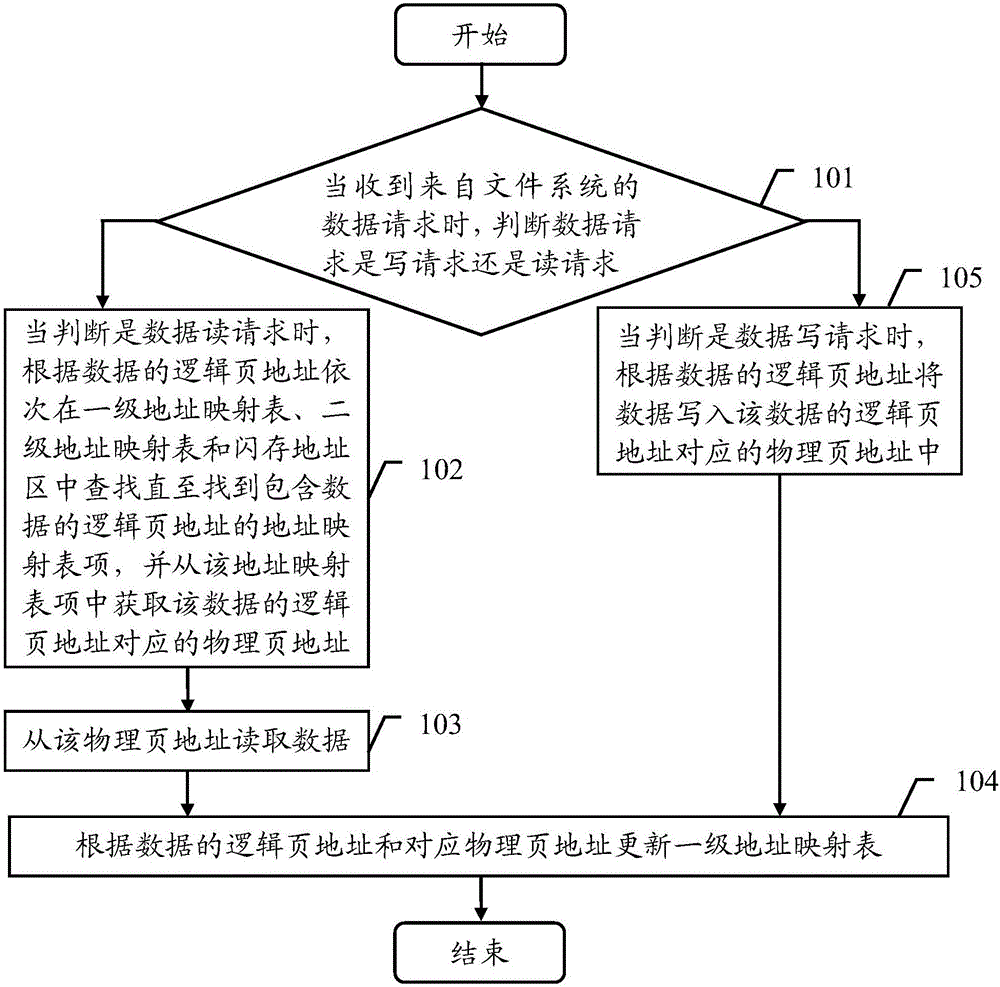
[0031] see figure 1 , is a schematic flowchart of the address mapping method of the flash memory storage system in the first embodiment of the present invention. Such as figure 1 As shown, the address mapping method of the flash memory storage system provided by the embodiment of the present invention includes the following steps:

[0032]...


PUM


Abstract

Embodiments of the invention disclose an address mapping method and apparatus for a flash storage system. The method comprises the steps of judging whether a data request from a file system is a write request or a read request; when the data request is judged to be the read request, accessing a first-level address mapping table preset in a cache, a second-level address mapping table preset in a memory and a flash address region in sequence according to a logic page address of data until a corresponding address mapping table item is found and a corresponding physical page address is obtained from the address mapping table item, then reading the data from the physical page address, and updating the first-level address mapping table according to the logic page address and the physical page address of the data; and when the data request is judged to be the write request, writing the data in the physical page address according to the logic page address of the data, and updating the first-level address mapping table according to the logic page address and the physical page address of the data. By adopting the scheme, the memory space required for storing address mapping table items is greatly reduced, the read-write performance of the flash storage system can be effectively improved, and the system response time is shortened.

Description

technical field [0001] The invention belongs to the technical field of data storage, and in particular relates to an address mapping method and device for a flash memory storage system. Background technique [0002] With the development of semiconductor technology and computer architecture, flash memory storage system, as a non-volatile storage system, gradually replaces the traditional Electromagnetic storage devices are widely used in embedded systems. Embedded system is application-centric, based on computer technology, software and hardware can be tailored, and is suitable for special-purpose computer systems that have strict requirements on function, reliability, cost, volume, and power consumption. Among them, the storage system is an important part of the embedded system. At present, flash memory storage systems mainly include NAND and NOR. Due to the higher storage density and faster writing speed of NAND flash memory, flash memory storage systems based on NAND fla...

Claims


Application Information

Patent Timeline
Patent Type & Authority Applications(China)
IPC IPC(8): G06F12/02
CPCG06F12/0246G06F2212/7201
Inventor 席爱民
Owner 深圳市先天海量技术有限公司
Why Eureka
Try Eureka