Organic light-emitting diode (OLED) display panel and display device

A display panel and display device technology, which is applied in the direction of static indicators, instruments, electrical components, etc., can solve the problems of restricting resolution, etc., and achieve the effect of reducing the difficulty of the process, reducing the requirements of the arrangement density, and reducing the manufacturing process and coating process

Pending Publication Date: 2017-10-13
WUHAN CHINA STAR OPTOELECTRONICS SEMICON DISPLAY TECH CO LTD
View PDF11 Cites 6 Cited by
  • Summary
  • Abstract
  • Description
  • Claims
  • Application Information

AI Technical Summary

Problems solved by technology

In the current mainstream RGB Stripe and Pentile arrangements, each sub-pixel corresponds to an opening of the metal mask. In order to avoid color aliasing, the distance between the openings of different color sub-pixels has a minimum limit, which restricts the resolution. Further improve

Method used


Image

  • Organic light-emitting diode (OLED) display panel and display device
  • Organic light-emitting diode (OLED) display panel and display device
  • Organic light-emitting diode (OLED) display panel and display device

Examples


Embodiment Construction

[0028] The following descriptions of the various embodiments refer to the accompanying drawings to illustrate specific embodiments in which the invention may be practiced. The directional terms mentioned in the present invention, such as [top], [bottom], [front], [back], [left], [right], [inside], [outside], [side], etc., are only for reference The orientation of the attached schema. Therefore, the directional terms used are used to illustrate and understand the present invention, but not to limit the present invention. In the figures, structurally similar elements are denoted by the same reference numerals.

[0029] The present invention aims at the existing OLED display panel, which is limited by the manufacturing process of the mask plate and the coating process, which leads to the problem that the display effect of the OLED cannot be further improved, etc., and proposes an OLED display panel. This embodiment can solve this problem .

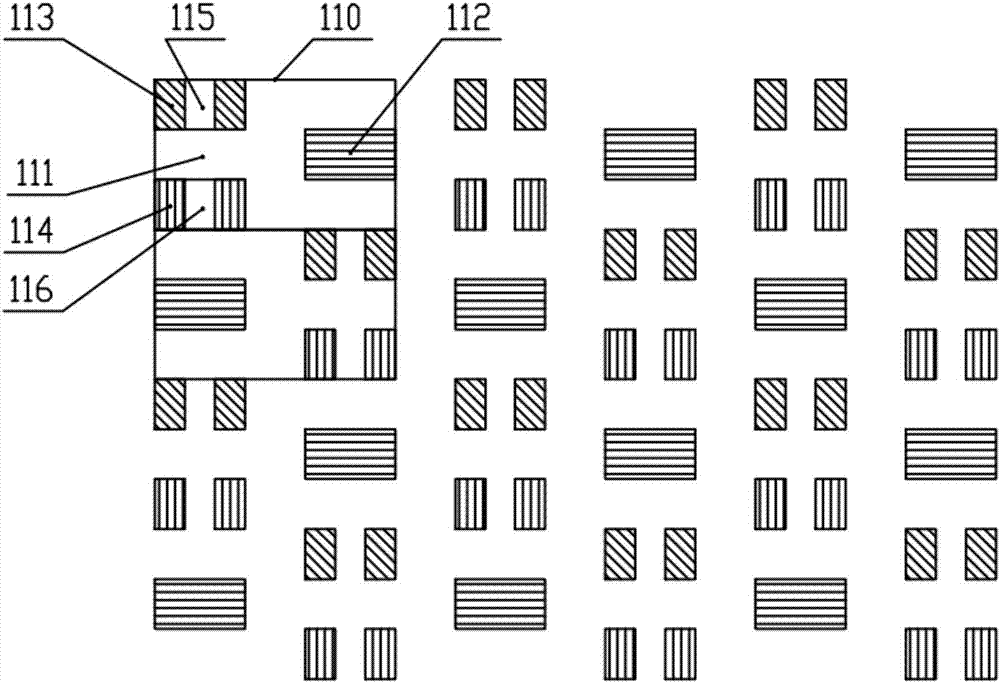
[0030] figure 1 Shown is a schemat...


PUM


Abstract

The invention provides an organic light-emitting diode (OLED) display panel and a display device. The OLED display panel comprises at least two pixel group units, wherein the at least two pixel group units are arranged along a first direction or a second direction, each pixel group unit comprises two sub-pixel group units arranged along the second direction, each sub-pixel group unit comprises a first sub-pixel, a second sub-pixel and a third sub-pixel, two adjacent second sub-pixels form a second sub-pixel group, two adjacent third sub-pixels form a third sub-pixel group, and arbitrary three adjacent first sub-pixels, arbitrary three adjacent second sub-pixels and arbitrary three adjacent third sub-pixels form a basic pixel unit. The OLED display panel has the beneficial effects that adjacent sub-pixels or sub-pixel groups are shared by the sub-pixels, so that the OLED display quality and effect are improved on the same number of sub-pixels, or the requirement on sub-pixel arrangement density of a display is reduced on the condition that the same sensing resolution is maintained unchanged.

Description

technical field [0001] The invention relates to the field of display technology, in particular to an OLED display panel and a display device. Background technique [0002] In flat panel display technology, Organic Light-Emitting Diode (OLED) display has many advantages such as thinness, active light emission, fast response speed, large viewing angle, wide color gamut, high brightness and low power consumption, etc., and has gradually become the successor. The third generation display technology after liquid crystal display. Compared with LCD (Liquid crystal displays, liquid crystal display), OLED has the advantages of saving power, being thinner, and having a wider viewing angle, which is incomparable to LCD. At present, people have higher and higher requirements for the fineness of the display, that is, the resolution, but the production of high-quality, high-resolution OLED displays still faces many challenges. [0003] At present, in terms of device manufacturing, the m...

Claims


Application Information

Patent Timeline
IPC IPC(8): H01L27/32
CPCH10K59/353G09G3/3208G09G2300/0452
Inventor 孙亮田念张耀仁
Owner WUHAN CHINA STAR OPTOELECTRONICS SEMICON DISPLAY TECH CO LTD
Why Eureka
Try Eureka