Display panel and manufacturing method thereof

A display panel and manufacturing method technology, applied in the direction of instruments, nonlinear optics, optics, etc., can solve the problems of large differences in display effects of liquid crystal display panels, achieve uniform force, and reduce the effect of display effect differences

Active Publication Date: 2020-04-28
BOE TECH GRP CO LTD +1
View PDF9 Cites 0 Cited by
  • Summary
  • Abstract
  • Description
  • Claims
  • Application Information

AI Technical Summary

Problems solved by technology

[0005] The present invention provides a display panel and a manufacturing method thereof, which can solve the difference between the display effect of the liquid crystal display panel cut from the peripheral area of ​​the liquid crystal mother board and the display effect of the liquid crystal display panel cut from the central area of ​​the liquid crystal mother board big problem

Method used


Image

  • Display panel and manufacturing method thereof
  • Display panel and manufacturing method thereof
  • Display panel and manufacturing method thereof

Examples


Embodiment Construction

[0058] In order to make the purpose, technical solutions and advantages of the present invention clearer, the present invention will be further described in detail below in conjunction with the accompanying drawings. Obviously, the described embodiments are only some of the embodiments of the present invention, rather than all of them. Based on the embodiments of the present invention, all other embodiments obtained by persons of ordinary skill in the art without making creative efforts belong to the protection scope of the present invention.

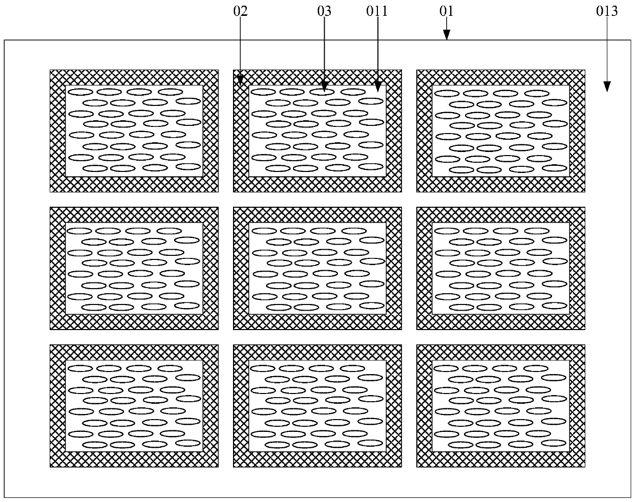
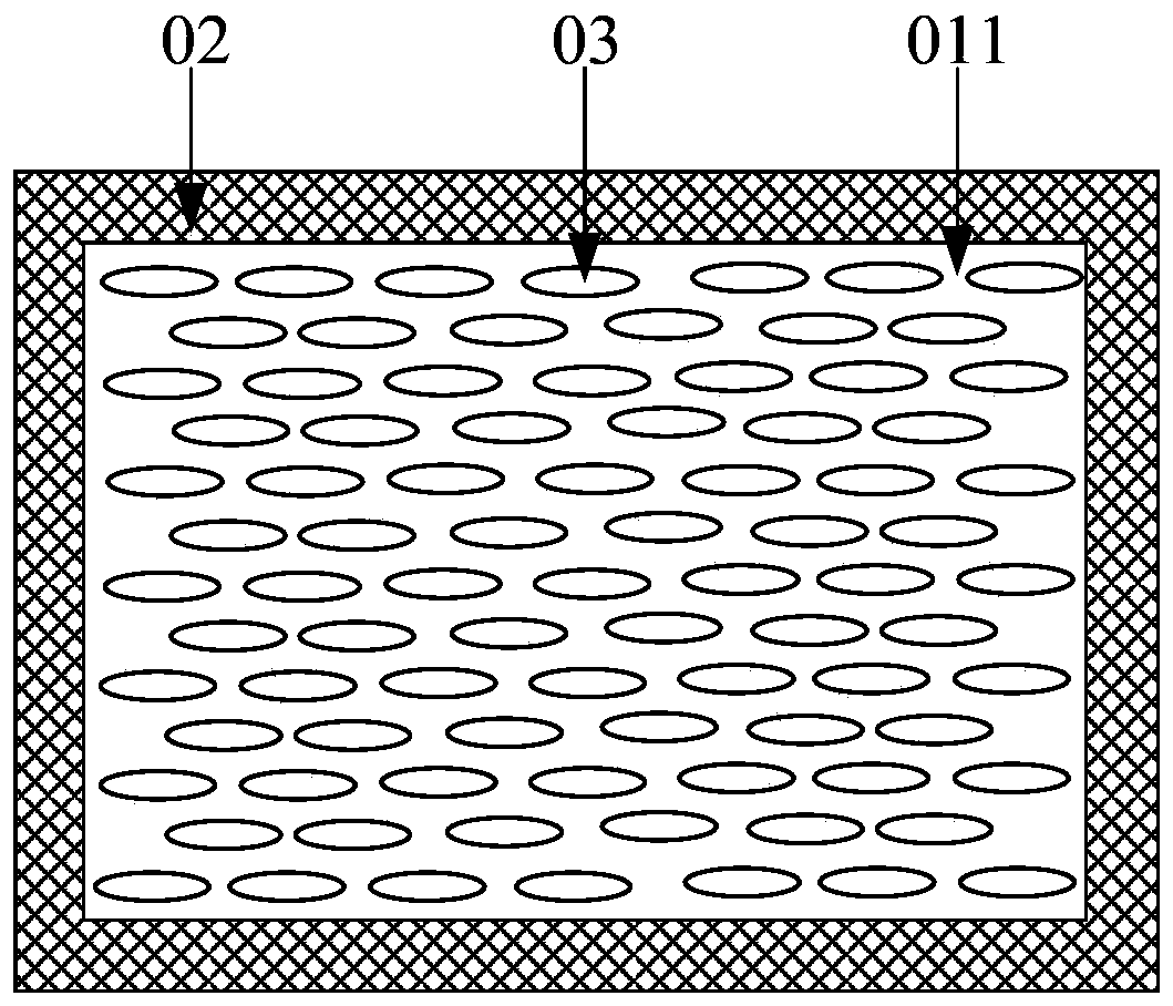
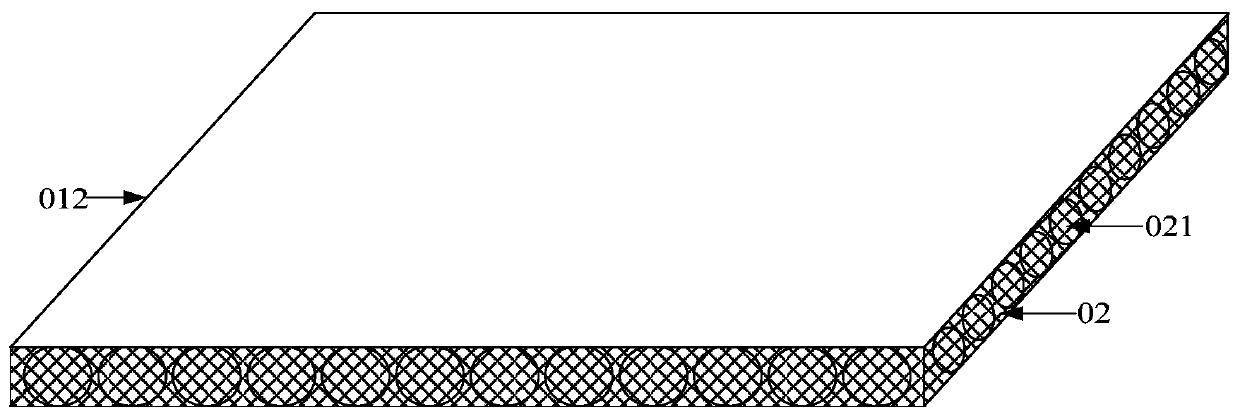
[0059] Thin Film Transistor-Liquid Crystal Display (English: Thin Film Transistor-Liquid Crystal Display; abbreviation: TFT-LCD) includes a liquid crystal display panel. The liquid crystal display panel includes an array substrate and a color filter substrate formed in a box, and an array substrate and a color filter substrate. Liquid crystal and frame sealant, the frame sealant can bond the array substrate and the color filter substrate...


PUM

PropertyMeasurementUnit
diameteraaaaaaaaaa

Abstract

The invention discloses a display panel and a manufacturing method thereof, belonging to the technical field of display. The method includes: coating a sealant on the peripheral area of ​​each liquid crystal region of the first motherboard, the sealant is doped with a supporting structure, and the plurality of liquid crystal regions of the first motherboard include a liquid crystal region located in the center of the first motherboard The central liquid crystal region of the area and the first liquid crystal region located in the first peripheral region of the first motherboard, the height of the support structure doped in the sealant coated in the peripheral region of the first liquid crystal region is higher than that coated in the central liquid crystal region The height of the support structure doped in the sealant in the peripheral area of ​​the region; the second mother board is arranged opposite to the first mother board to obtain a liquid crystal mother board, and liquid crystals are arranged in each liquid crystal region. The invention solves the problem that the display effects of different display panels cut from the liquid crystal mother board have large differences in display effects, and helps to reduce the difference in display effects of different display panels cut from the liquid crystal mother board.

Description

technical field [0001] The invention relates to the field of display technology, in particular to a display panel and a manufacturing method thereof. Background technique [0002] The liquid crystal display panel includes an array substrate and a color filter substrate formed in a box, and a liquid crystal and a sealant between the array substrate and the color filter substrate. The orthographic projection of the sealant on the array substrate is located in the peripheral area of ​​the array substrate. It is located in the space enclosed by the sealing glue. [0003] The liquid crystal display panel is a display panel formed by cutting a liquid crystal mother board, and the liquid crystal mother board is formed by pairing an array mother board and a color filter mother board. The array mother board includes a plurality of liquid crystal regions. During the manufacturing process of the liquid crystal display panel, firstly, a sealant is coated on the peripheral region of eac...

Claims


Application Information

Patent Timeline
Patent Type & Authority Patents(China)
IPC IPC(8): G02F1/1333G02F1/1339
CPCG02F1/133351G02F1/13394G02F1/1339G02F1/133354G02F1/133391G02F1/133325G02F1/13396
Inventor 张磊胡鹏举张晓峰王长全
Owner BOE TECH GRP CO LTD
Why Eureka
Try Eureka