Fingerprint identification chip package structure and packaging method

A technology of fingerprint identification and packaging structure, which is applied in the direction of character and pattern recognition, instruments, electrical components, etc., and can solve the problems of reducing the accuracy of fingerprint identification and optical signal crosstalk

Inactive Publication Date: 2018-05-11
CHINA WAFER LEVEL CSP
View PDF10 Cites 9 Cited by
  • Summary
  • Abstract
  • Description
  • Claims
  • Application Information

AI Technical Summary

Problems solved by technology

Preparing so many pixels for a fingerprint recognition that is pressed by only one finger can easily lead to crosstalk between adjacent pixels and reduce the accuracy of fingerprint recognition

Method used


Image

  • Fingerprint identification chip package structure and packaging method
  • Fingerprint identification chip package structure and packaging method
  • Fingerprint identification chip package structure and packaging method

Examples


Embodiment Construction

[0124] The following will clearly and completely describe the technical solutions in the embodiments of the present invention with reference to the accompanying drawings in the embodiments of the present invention. Obviously, the described embodiments are only some, not all, embodiments of the present invention. Based on the embodiments of the present invention, all other embodiments obtained by persons of ordinary skill in the art without making creative efforts belong to the protection scope of the present invention.

[0125] In order to make the above objects, features and advantages of the present invention more comprehensible, the present invention will be further described in detail below in conjunction with the accompanying drawings and specific embodiments.

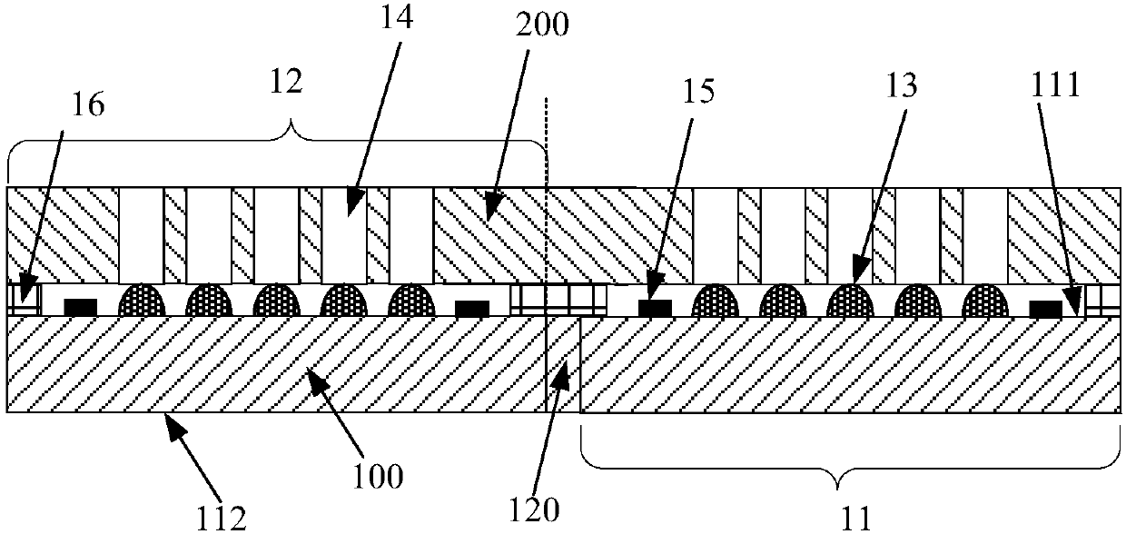
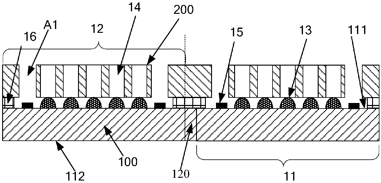
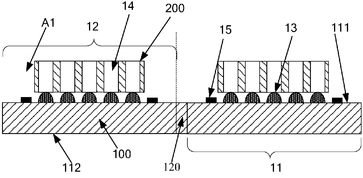
[0126] refer to Figure 1a , Figure 1a It is a structural schematic diagram of a package structure of a fingerprint identification chip provided by an embodiment of the present invention. The package structure inc...


PUM


Abstract

The invention discloses a fingerprint identification chip package structure and a packaging method. The package structure comprises a fingerprint identification chip, wherein the fingerprint identification chip comprises a first surface and a second surface, which are opposite, the first surface having a plurality of pixel points for collecting fingerprint information; and a semiconductor cover plate covered on the first surface, wherein the semiconductor cover plate has a plurality of through holes, the bottom portions of the through holes exposing the pixel points respectively. According tothe technical scheme, the first surface of the fingerprint identification chip is provided with the semiconductor cover plate, the semiconductor cover plate has the plurality of through holes in one-to-one correspondence with the pixel points of fingerprint identification chip respectively, and the through holes are used for exposing the pixel points, so that the problem of crosstalk between adjacent pixel points can be reduced, and fingerprint identification accuracy is improved.

Description

[0001] This application claims the priority of the Chinese patent application with the application number 201710034991.9 and the title of the invention "a packaging structure and packaging method for a fingerprint identification chip" submitted to the China Patent Office on January 17, 2017, the entire contents of which are incorporated by reference in this application. [0002] This application claims the priority of the Chinese patent application with the application number 201720053790.9 and the utility model name "a packaging structure for a fingerprint identification chip" submitted to the China Patent Office on January 17, 2017, the entire contents of which are incorporated herein by reference. Applying. [0003] This application claims the priority of the Chinese patent application with the application number 201720141464.3 and the utility model name "Fingerprint Identification Chip Packaging Structure" submitted to the China Patent Office on February 16, 2017, the entire...

Claims


Application Information

Patent Timeline
Patent Type & Authority Applications(China)
IPC IPC(8): H01L23/498H01L23/31H01L21/56
CPCH01L23/498H01L21/56H01L23/3114H01L23/31H01L2224/48091H01L2224/73265G06F18/00H01L2924/00014
Inventor 王之奇
Owner CHINA WAFER LEVEL CSP
Why Eureka
Try Eureka