A quantum dot display panel and three-dimensional printing device

A technology for display panels and 3D printing, which is applied in semiconductor devices, electrical components, additive processing, etc.

Active Publication Date: 2021-01-19
SHANGHAI AVIC OPTOELECTRONICS
View PDF6 Cites 0 Cited by
  • Summary
  • Abstract
  • Description
  • Claims
  • Application Information

AI Technical Summary

Problems solved by technology

[0005] The invention provides a quantum dot display panel and a three-dimensional printing device to reduce the brightness of the display panel in the dark state and solve the problem of photosensitive resin corresponding to the non-effective graphic area

Method used


Image

  • A quantum dot display panel and three-dimensional printing device
  • A quantum dot display panel and three-dimensional printing device
  • A quantum dot display panel and three-dimensional printing device

Examples


Embodiment Construction

[0022] The present invention will be further described in detail below in conjunction with the accompanying drawings and embodiments. It should be understood that the specific embodiments described here are only used to explain the present invention, but not to limit the present invention. In addition, it should be noted that, for the convenience of description, only some structures related to the present invention are shown in the drawings but not all structures.

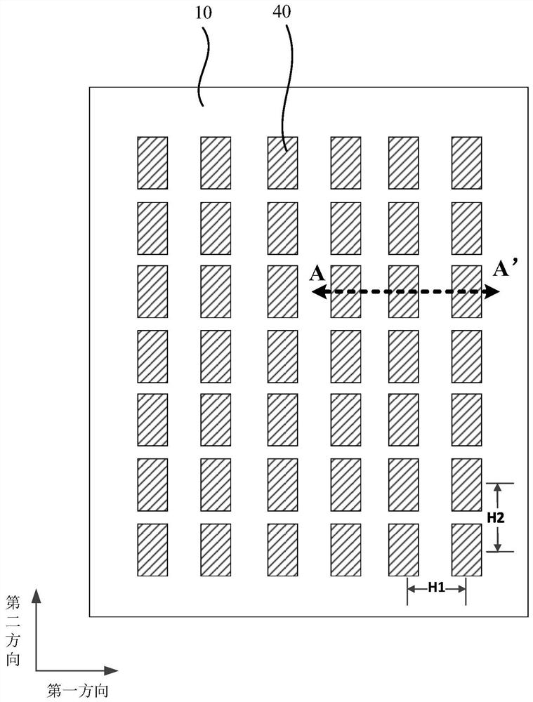
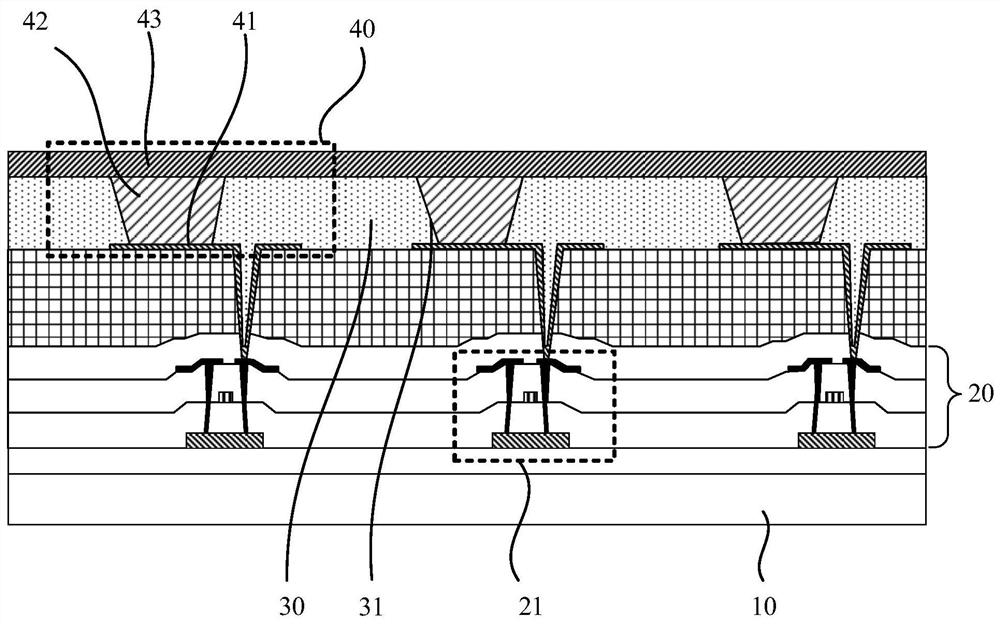
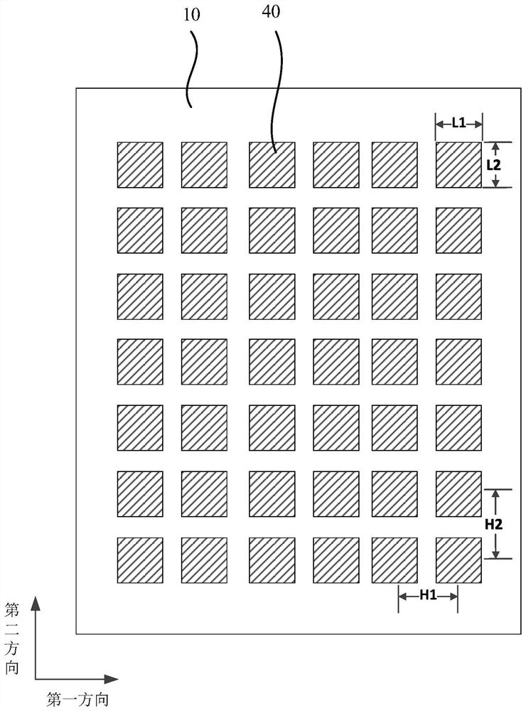
[0023] figure 1 It is a schematic diagram of a top view structure of a quantum dot display panel provided by an embodiment of the present invention, figure 2 for along figure 1 Schematic diagram of the cross-sectional structure in the direction of AA', combined with figure 1 and figure 2 As shown, the quantum dot display panel includes a substrate 10 , a control circuit layer 20 , a pixel definition layer 30 and a plurality of light emitting units 40 . The control circuit layer 20 is located on one side of t...


PUM

PropertyMeasurementUnit
wavelengthaaaaaaaaaa
emission peakaaaaaaaaaa

Abstract

The present invention provides a quantum dot display panel and a three-dimensional printing device. The quantum dot display panel includes: a substrate; a control circuit layer located on one side of the substrate, and the control circuit layer includes a plurality of control circuits; a pixel definition layer and A plurality of light-emitting units are located on the side of the control circuit layer away from the substrate; the pixel definition layer includes a plurality of openings, and the plurality of light-emitting units are respectively located in the openings; the control circuit is electrically connected to the light-emitting A unit for controlling the light-emitting state of the light-emitting unit; any of the light-emitting units sequentially includes a first electrode, a quantum dot light-emitting layer, and a second electrode in a direction away from the substrate; the light emitted by the light-emitting unit The wavelength is between 350nm and 450nm. The invention provides a quantum dot display panel and a three-dimensional printing device to reduce the brightness of the display panel in a dark state and solve the problem of photosensitive resin corresponding to the non-effective pattern area.

Description

technical field [0001] The invention relates to the field of display technology, in particular to a quantum dot display panel and a three-dimensional printing device. Background technique [0002] Rapid prototyping technology, also known as three-dimensional printing (3D printing), is a high-tech manufacturing technology based on material accumulation method. According to the three-dimensional model data of parts or objects, physical objects or Mock-up. Due to the advantages of greatly reducing production costs, improving the utilization of raw materials and energy, customizing according to needs, and greatly saving product production time, 3D printing technology has gradually entered the public eye and developed rapidly in recent years. [0003] The basic principle of 3D printing is layered processing and superimposed molding, that is, to generate 3D entities by adding materials layer by layer. When 3D printing is performed, the computer first obtains the 3D model of the o...

Claims


Application Information

Patent Timeline
Patent Type & Authority Patents(China)
IPC IPC(8): H01L27/32H01L51/56B29C64/20B33Y30/00
CPCB33Y30/00H10K59/121H10K71/135
Inventor 敦栋梁王臣夏志强刘金娥秦锋
Owner SHANGHAI AVIC OPTOELECTRONICS
Why Eureka
Try Eureka