Liquid crystal display panel and manufacturing method thereof

A liquid crystal display and panel technology, which is applied in the direction of instruments, nonlinear optics, optics, etc., can solve the problems of reducing the effective display area of ​​the display area and contaminating the liquid crystal with sealing glue, so as to improve the display effect of the screen, improve the display quality and performance indicators , Reduce the effect of dark state brightness

Active Publication Date: 2015-08-12
BOE TECH GRP CO LTD
View PDF5 Cites 0 Cited by
  • Summary
  • Abstract
  • Description
  • Claims
  • Application Information

AI Technical Summary

Problems solved by technology

[0006] The primary technical problem to be solved in the present invention is how to avoid the influence of external temperature, humidity and other factors on the sealing glue, and then pollute the liquid crystal through the sealing glue; the further technical problem to be solved is how to avoid the direct contact between the sealing glue and the liquid crystal , affect the liquid crystal arrangement and contaminate the liquid crystal, and will not reduce the effective display area of ​​the display area and affect the viewing effect

Method used


Image

  • Liquid crystal display panel and manufacturing method thereof
  • Liquid crystal display panel and manufacturing method thereof
  • Liquid crystal display panel and manufacturing method thereof

Examples


Embodiment 1

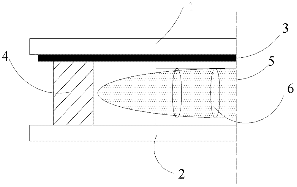
[0032] The liquid crystal display panel includes an upper substrate group and a lower substrate group, spacers are arranged between the two substrate groups, the surrounding frames of the two substrate groups are bonded by frame sealant, and liquid crystal is filled between the two substrate groups. Figure 5 Shows a schematic diagram of the peripheral structure of the liquid crystal display panel of this embodiment, where the upper substrate group is a color filter substrate 1, the lower substrate group is an array substrate 2, and the color filter substrate 1 is provided with a black matrix 3, and the color filter substrate 1 And the array substrate 2 is also provided with a liquid crystal alignment layer (not shown in the figure), the spacer 6 is arranged between the liquid crystal alignment layers, and an inner isolation layer 11 and an outer isolation layer 12 are arranged on the periphery of the two substrates, and the frame is sealed The glue 4 is coated between the inner...

Embodiment 2

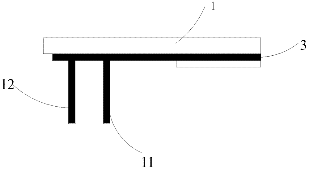
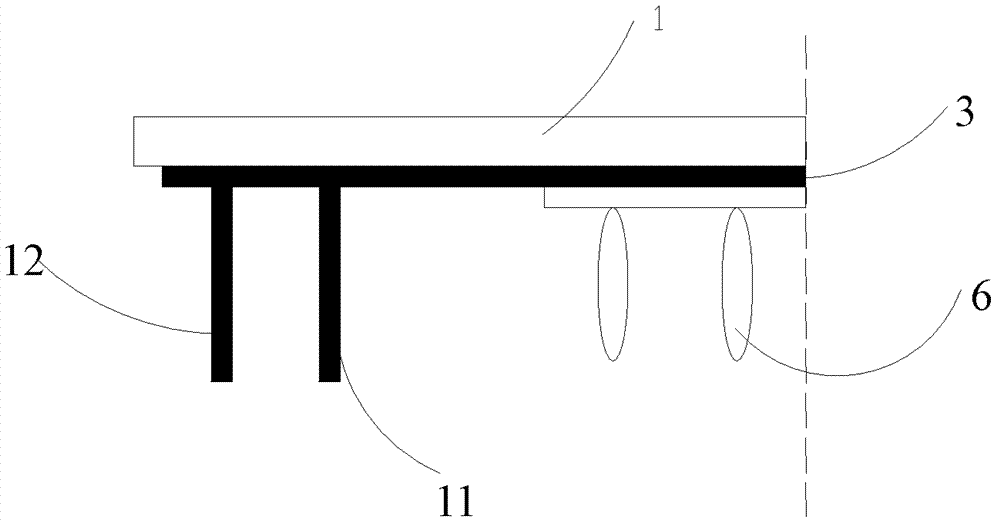
[0038] The structure of the liquid crystal display panel of this embodiment is similar to the structure of the liquid crystal display panel described in Embodiment 1, with the difference that the isolation layer is only provided on the outside of the frame sealant to isolate the frame sealant from the external environment and avoid The external environment will cause corrosion, peeling or disconnection of the frame sealant. At the same time, it can also block the backlight from entering the peripheral area of ​​the LCD panel, reduce the brightness in the dark state, and improve the contrast.

Embodiment 3

[0040] In this embodiment, the upper substrate group of the liquid crystal display panel is a color filter substrate with a black matrix and the lower substrate group is an array substrate as an example to introduce the manufacturing process of the liquid crystal display panel. The difference between the manufacturing process of the liquid crystal display panel of this embodiment and the manufacturing process of the liquid crystal display panel in the prior art is that before the frame sealant is applied between the color film substrate and the array substrate constituting the liquid crystal display panel, An inner isolation layer and an outer isolation layer are prepared on a substrate, so that the inner isolation layer and the outer isolation layer are in contact with the color filter substrate and the array substrate, and the sealant is coated between the inner isolation layer and the outer isolation layer.

[0041] The specific manufacturing process of the liquid crystal displ...


PUM


Abstract

The invention belongs to the technical field of liquid crystal, and discloses a liquid crystal display panel. The liquid crystal display panel comprises an upper substrate group and a lower substrate group; a spacer is arranged between the two substrate groups; the frames around the two substrate groups are adhered by frame sealing glue; and liquid crystal is filled between the two substrate groups. The liquid crystal display panel is characterized in that at least outer side of the frame sealing glue is provided with an isolation layer. The invention further discloses a manufacturing method of the liquid crystal display panel. According to the scheme provided by the invention, the external isolation layer can isolate from an external condition, so as to avoid the situation that the frame sealing glue falls off and is broken due to the corrosion on the frame sealing glue, caused by conditions of external temperature and external moisture; an inner isolation layer can isolate the liquid crystal, so as to avoid the pollution on the liquid crystal; the box thicknesses at the periphery of the liquid crystal display are supported by the isolation layers, so that the box thicknesses of the liquid crystal display panel are the same; and furthermore, when the isolation layers are made of a material which is the same as a material of a black matrix, the peripheral light is shielded; the dark-state luminance is reduced; and the liquid crystal contrast ratio is improved to a certain extent.

Description

Technical field [0001] The present invention relates to the field of display technology, in particular to a liquid crystal display panel and a manufacturing method thereof. Background technique [0002] Liquid crystal displays dominate the flat panel display market. Liquid crystal displays are generally used as display screens of electronic products because of their light and thin characteristics, low power consumption and almost no radiation. At present, thin film transistor liquid crystal display (TFT-LCD) is the fastest growing technology in displays. The thin film transistor liquid crystal display mainly consists of three parts: the liquid crystal display panel, the backlight part and the driving part. Among them, the liquid crystal display panel is the part directly presented in front of people, and it directly reflects the overall quality of the liquid crystal display. Therefore, the manufacturing process of the liquid crystal display panel is extremely important. [0003...

Claims


Application Information

Patent Timeline
Patent Type & Authority Patents(China)
IPC IPC(8): G02F1/1333G02F1/1339G02F1/1337
Inventor 孙韬
Owner BOE TECH GRP CO LTD
Why Eureka
Try Eureka