Manufacturing method of semiconductor device

a manufacturing method and semiconductor technology, applied in solid-state devices, chemical vapor deposition coatings, reaction chambers of plasma cvd apparatuses, etc., can solve the problems of degradation of quality or uneven thickness of thin film formed over glass substrates, uneven surface standing wave effect, and uneven thickness of thin film. , to achieve the effect of improving the contrast of the display panel, high quality and favorable switching characteristics

Inactive Publication Date: 2009-02-19
SEMICON ENERGY LAB CO LTD
View PDF6 Cites 19 Cited by
  • Summary
  • Abstract
  • Description
  • Claims
  • Application Information

AI Technical Summary

Benefits of technology

[0046]In the thin film transistor which is obtained as described above, when it is turned on, a region near an interface with the gate insulating film in the microcrystalline silicon film with high quality which is formed under the first film formation condition serves as a channel formation region. When the thin film transistor is turned off, a groove which is obtained by etching a part of the buffer layer serves as a path where a very small amount of a leak current flows. Accordingly, compared to a conventional thin film transistor including a single amorphous silicon layer or a conventional thin film transistor including a single microcrystalline silicon layer, a ratio of off-current and on-current can be increased and switching characteristics are favorable, which lead to improvement in contrast of a display panel.
[0047]By generating plasma through supplying high-frequency power that does not exhibit an effect of surface standing wave and high-frequency power in the VHF band in accordance with a manufacturing method of the present invention, a semiconductor device using an even and good quality microcrystalline semiconductor film as a channel-forming region can be manufactured over a large-area glass substrate with a long side that has a length of 2000 mm. A thin film transistor that is obtained can have an electron field-effect mobility that is greater than 1 and less than or equal to 50. Therefore, a thin film transistor using the microcrystalline semiconductor film which is obtained according to the manufacturing method of the present invention has a current-voltage characteristic represented by a curve with a steep slope in a rising portion, has an excellent response as a switching element, and can be operated at high speed.
[0048]A light-emitting device using the thin film transistor that is obtained according to the manufacturing method of the present invention can suppress variation in threshold voltage of thin film transistors, which leads to improvement in reliability.
[0049]In addition, a liquid crystal display device using the thin film transistor which is obtained according to the manufacturing method of the present invention can increase field-effect mobility and thus can increase a driving frequency of a driver circuit. Since he driver circuit can be operated at high speed, a frame frequency can be quadruplicated or black frame insertion can be realized

Problems solved by technology

In such cases, the effect of a surface standing wave becomes very pronounced and the plasma density distribution in a reaction chamber of the plasma CVD apparatus becomes uneven.
Consequently, a problem such as degradation of quality or unevenness of thickness of a thin film formed over the glass substrate occurs.

Method used


Image

  • Manufacturing method of semiconductor device
  • Manufacturing method of semiconductor device
  • Manufacturing method of semiconductor device

Examples


embodiment mode 1

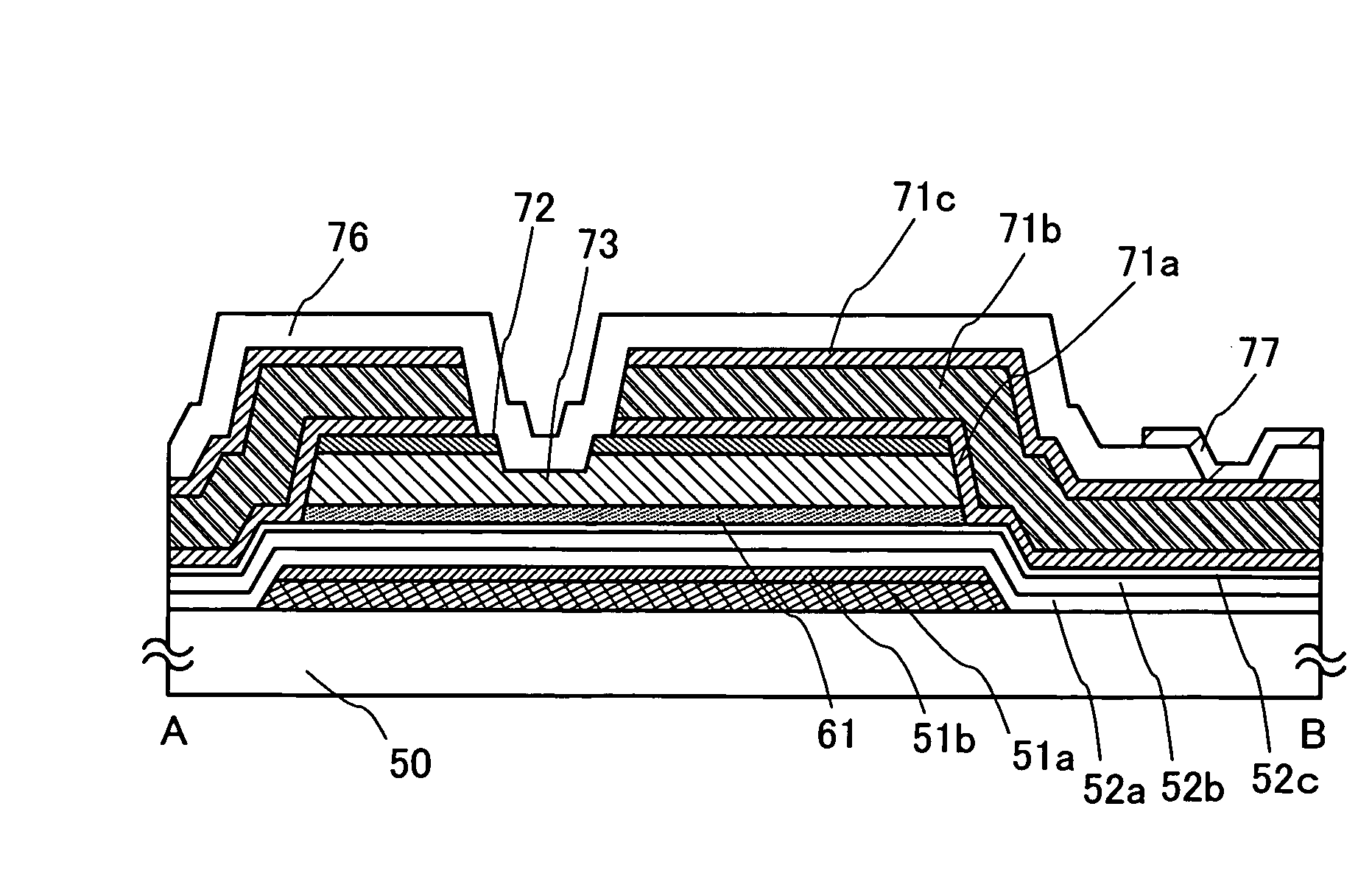
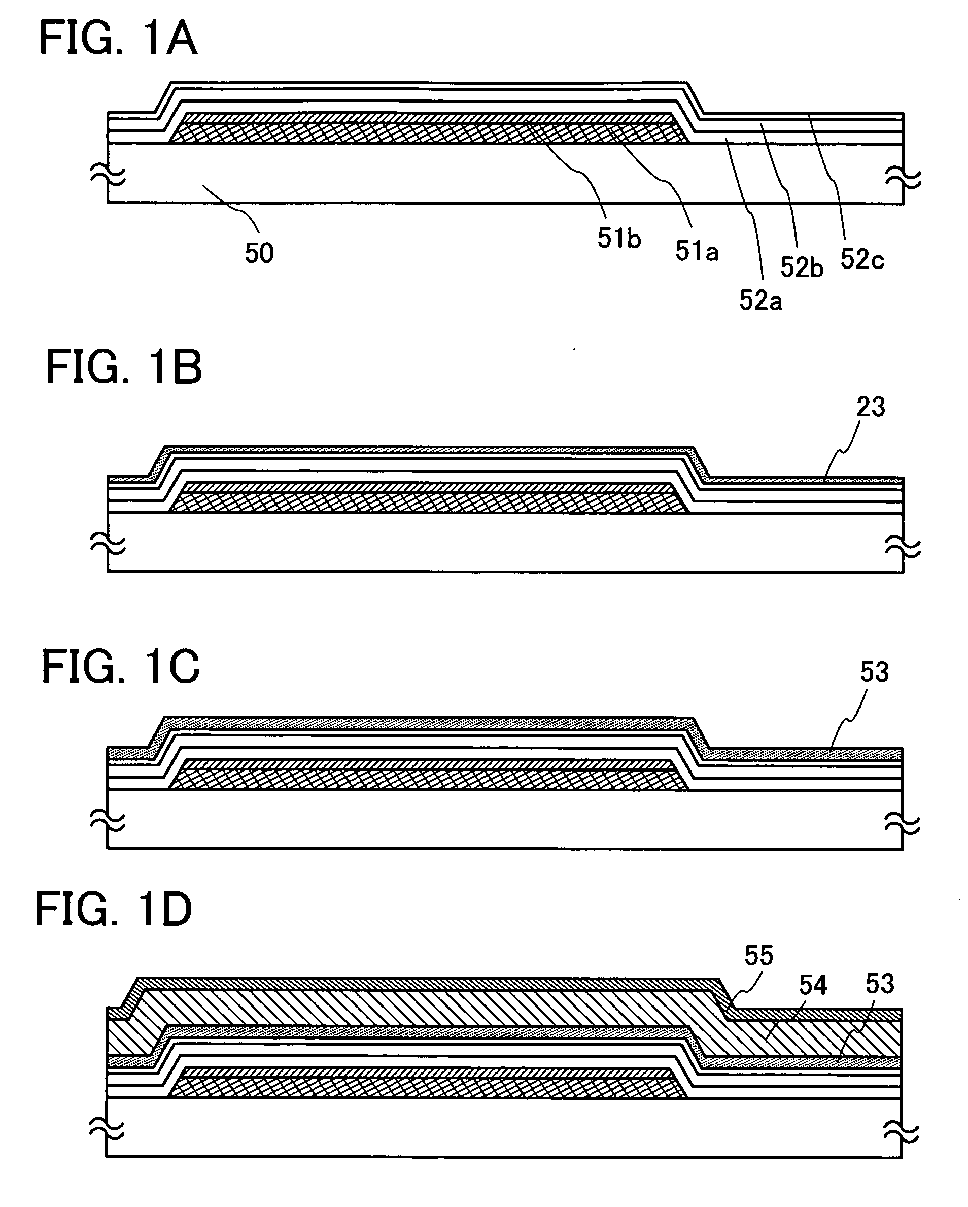
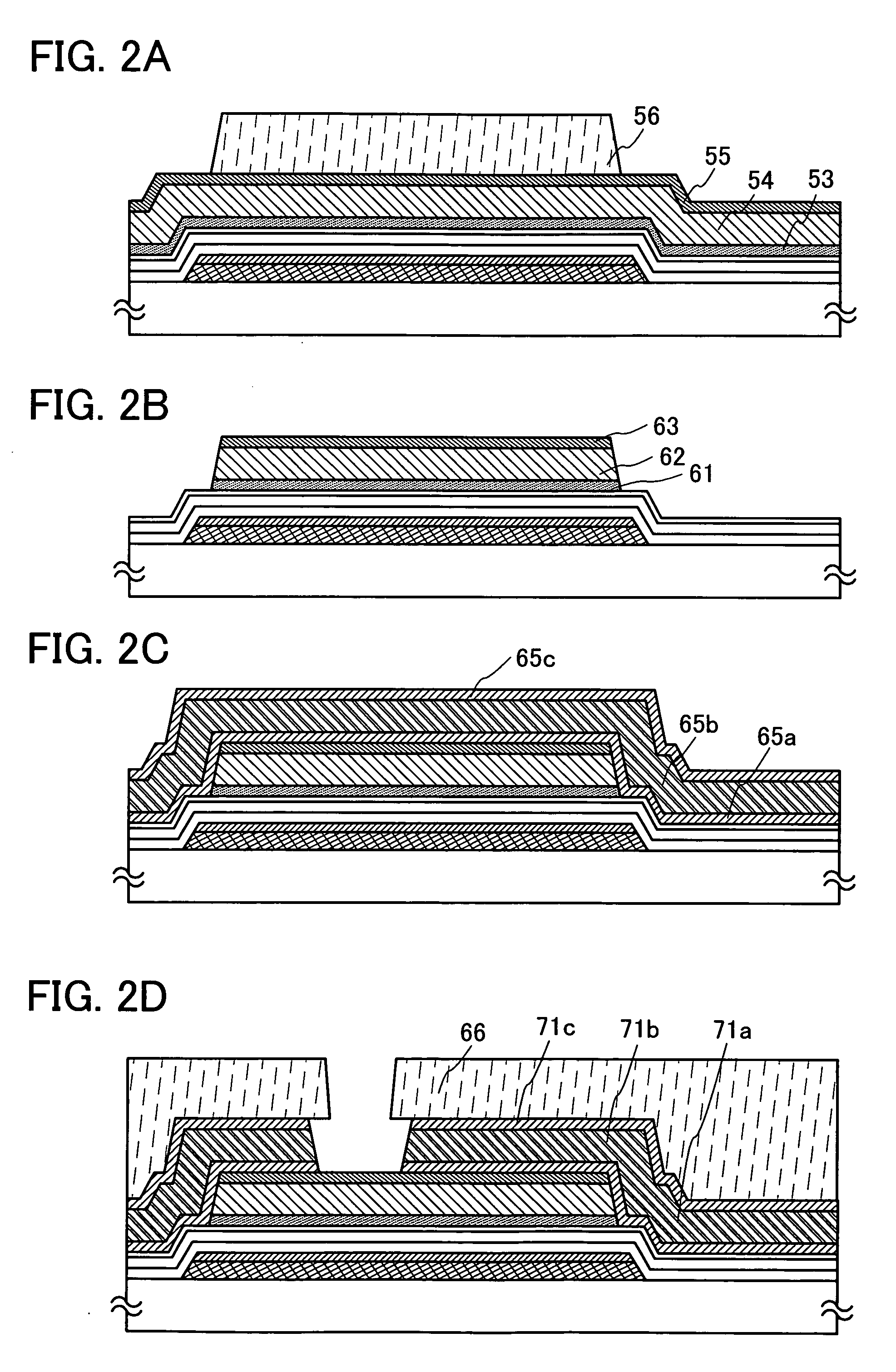
[0090]In this embodiment mode, a manufacturing process of a thin film transistor used for a liquid crystal display device is described with reference to FIGS. 1A to 1D, FIGS. 2A to 2D, FIGS. 3A to 3C, FIG. 4, FIG. 5, and FIG. 6. FIGS. 1A to 1D, FIGS. 2A to 2D, and FIGS. 3A to 3C are cross-sectional views showing a manufacturing process of a thin film transistor, and FIG. 4 is a top view showing a connection region of a thin film transistor and a pixel electrode in a single pixel. Further, FIG. 5 is a timing chart showing a formation method of a microcrystalline silicon film, and FIG. 6 is a cross-sectional view showing a structural example of a plasma CVD apparatus capable of generating glow discharge plasma by supplying two or more kinds of high-frequency powers with different frequencies.

[0091]An n-channel thin film transistor having a microcrystalline semiconductor film is more suitable for use in a driver circuit than a p-channel thin film transistor having a microcrystalline se...

embodiment mode 2

[0165]This embodiment mode shows an example of a multi-chamber plasma CVD apparatus suitable for formation of a gate insulating film, a microcrystalline semiconductor film, and an n+layer included in the TFT described in Embodiment Mode 1.

[0166]FIG. 10 shows one example of a multi-chamber plasma CVD apparatus provided with a plurality of reaction chambers. This apparatus is provided with a common chamber 123, a load / unload chamber 122, a first reaction chamber 100a, a second reaction chamber 100b, and a third reaction chamber 100c. This apparatus is a single wafer-processing type in which a substrate set in a cassette 124 in the load / unload chamber 122 is transferred to / from each reaction chamber by a transfer unit 126 in the common chamber 123. A gate valve 125 is provided between the common chamber 123 and each reaction chamber, so that processing in one reaction chamber does not affect processing in other reaction chambers.

[0167]The reaction chambers are sorted according to the k...

embodiment mode 3

[0174]This embodiment mode will describe a manufacturing process of a thin film transistor using a multi-chamber CVD apparatus which is different from that in FIG. 11 described in Embodiment Mode 2, with reference to FIG. 11. FIG. 11 shows the apparatus provided with three reaction chambers, whereas FIG. 11 is a top view of a multi-chamber CVD apparatus provided with four reaction chambers.

[0175]FIG. 11 shows a structure in which a fourth reaction chamber 100d is provided in addition to the structure of the multi-chamber CVD apparatus of FIG. 10. In FIG. 11, the same components as in FIG. 10 are denoted by the same reference numerals and detailed description thereof is omitted. Further, a combination of exhaust units shown in FIG. 11 is one example and the combination is not particularly limited thereto.

[0176]A gas supply unit 108b is connected to the fourth reaction chamber 100d. The structure of the high-frequency power supply units and the exhaust units is the same as in FIG. 10....


PUM

PropertyMeasurementUnit
temperatureaaaaaaaaaa

Abstract

An object is to provide a manufacturing method of a microcrystalline semiconductor film with favorable quality over a large-area substrate. After forming a gate insulating film over a gate electrode, in order to improve quality of a microcrystalline semiconductor film formed in an initial stage, glow discharge plasma is generated by supplying high-frequency powers with different frequencies, and a lower part of the film near an interface with the gate insulating film is formed under a first film formation condition, which is low in film formation rate but results in a good quality film. Thereafter, an upper part of the film is deposited under a second film formation condition with higher film formation rate, and further, a buffer layer is stacked on the microcrystalline semiconductor film.

Description

BACKGROUND OF THE INVENTION[0001]1. Field of the Invention[0002]The present invention relates to a semiconductor device including a circuit, which is formed using a thin film transistor (hereinafter referred to as a TFT), and a manufacturing method thereof. For example, the present invention relates to an electronic device provided with, as a component, an electro-optical device typified by a liquid crystal display panel or a light-emitting display device having an organic light-emitting element.[0003]Note that in this specification, a semiconductor device refers to all types of devices which can function by utilizing semiconductor characteristics. An electro-optical device, a semiconductor circuit, and an electronic device are all included in the category of the semiconductor device.[0004]2. Description of the Related Art[0005]In recent years, a technique for forming thin film transistors (TFTs) using a semiconductor thin film (a thickness of several tens of nm to several hundred n...

Claims


Application Information

Patent Timeline
Patent Type & Authority Applications(United States)
IPC IPC(8): H01L21/00
CPCC23C16/509C23C16/515H01L29/04H01L27/1288H01L29/4908H01L29/78696H01L29/458H01L21/2053H01L29/66765
Inventor YAMAZAKI, SHUNPEITEDUKA, SACHIAKITORIUMI, SATOSHIFURUNO, MAKOTOJINBO, YASUHIRODAIRIKI, KOJIKUWABARA, HIDEAKI
Owner SEMICON ENERGY LAB CO LTD
Why Eureka
Try Eureka