How to make a display

A manufacturing method and display technology, applied in the direction of semiconductor devices, electrical solid devices, electrical components, etc., can solve the problems of high cost, low yield, difficult picking and alignment

Active Publication Date: 2020-11-17
PLAYNITRIDE
View PDF6 Cites 0 Cited by
  • Summary
  • Abstract
  • Description
  • Claims
  • Application Information

AI Technical Summary

Problems solved by technology

However, today’s displays usually have millions of pixels, and the small size of the light-emitting diode components makes it difficult to pick up and align accurately. LED display with color display effect, its cost is high, the process time is long and the yield rate is low

Method used


Image

  • How to make a display
  • How to make a display
  • How to make a display

Examples


Embodiment Construction

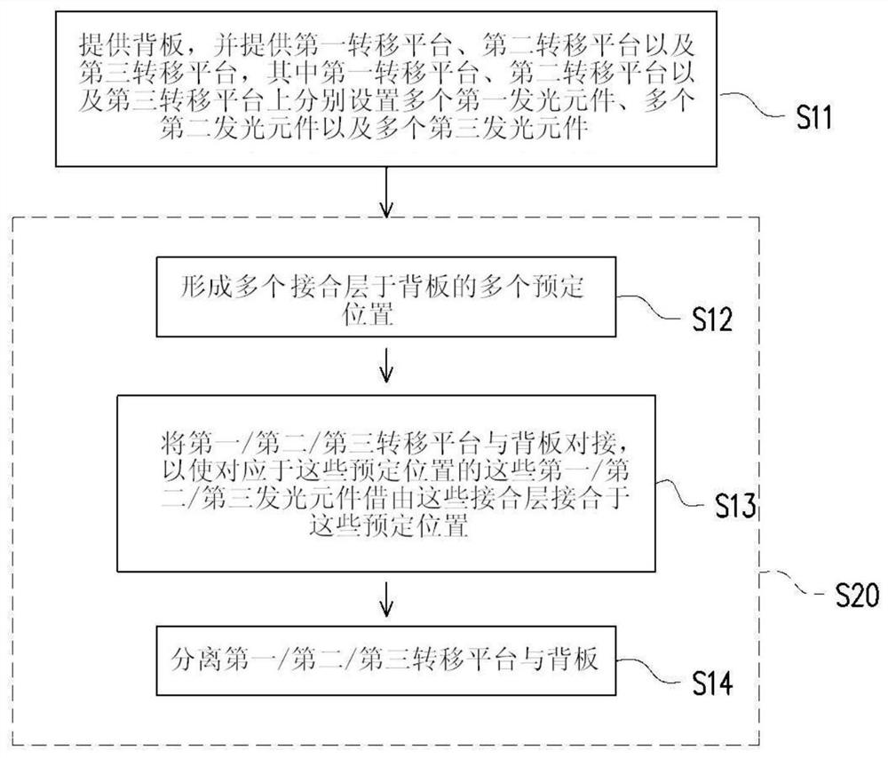
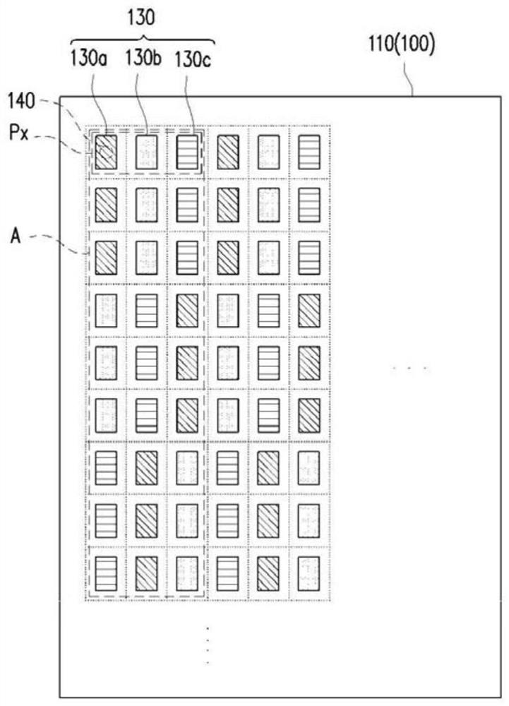
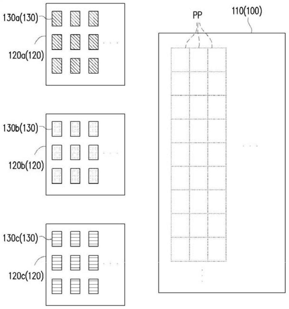
[0059] figure 1 A schematic flow chart showing the main steps of the manufacturing method of the display according to the first embodiment of the present invention, figure 2 A schematic top view of the display 100 fabricated in the first embodiment is then shown. in addition, image 3 Show the backplane 110 and the transfer platform 120 provided in the manufacturing method of the display in the first embodiment of the present invention, please refer to Figure 1 to Figure 3 . In the first embodiment, the manufacturing method of the display is described in detail below.

[0060] First, see figure 1 , image 3 , in step S11 , providing a backplane 110 and providing a plurality of transfer platforms 120 . In the first embodiment, there are multiple predetermined positions PP on the backplane 110 , and each predetermined position PP is, for example, a corresponding position of a sub-pixel of the display. These transfer platforms 120 include a first transfer platform 120a, ...


PUM

PropertyMeasurementUnit
lengthaaaaaaaaaa

Abstract

The invention provides a display making method. The making method comprises the following steps: a backplane, a first transfer platform and a second transfer platform are firstly provided, wherein multiple first light emitting modules are arranged on the first transfer platform, and multiple second light emitting modules are arranged on the second transfer platform; then, multiple first joint layers are formed at multiple first positions on the backplane, and later, the first transfer platform is in butt joint with the backplane to enable the first light emitting modules corresponding to the first positions to be joined at the first positions with the help of the first joint layers; then, multiple second joint layers are formed at multiple second positions on the backplane, and later, thesecond transfer platform is in butt joint with the backplane to enable the second light emitting modules corresponding to the second positions to be joined at the second positions with the help of thesecond joint layers. Thus, multiple light emitting modules with different colors can be quickly and accurately arranged on the backplane of the display, the display making cost is low, and the yieldis high.

Description

technical field [0001] The invention relates to a manufacturing method of a display, in particular to a manufacturing method of a light emitting diode display. Background technique [0002] With the advancement of optoelectronic technology, the volume of many optoelectronic components is gradually miniaturized. In recent years, due to breakthroughs in the size of light-emitting diodes (light-emitting diodes, LEDs), light-emitting diode (micro-LED) displays, which are made of light-emitting diodes arranged in arrays, are gradually gaining attention in the market. Light-emitting diode displays are active light-emitting component displays. In addition to saving power compared to organic light-emitting diode (OLED) displays, they also have better contrast performance and can be used in sunlight Has visibility. In addition, since the light-emitting diode display uses inorganic materials, it has better reliability and a longer service life than the organic light-emitting diode d...

Claims


Application Information

Patent Timeline
Patent Type & Authority Patents(China)
IPC IPC(8): H01L33/00H01L27/15
CPCH01L27/156H01L33/0095
Inventor 赖育弘林子旸罗玉云
Owner PLAYNITRIDE
Why Eureka
Try Eureka