

A kind of semiconductor wafer electroplating equipment
A technology for electroplating equipment and semiconductors, applied in electrolytic components, electrolytic processes, etc., can solve the problem of inconsistent wafer electroplating uniformity, and achieve the effect of improving adsorption effect, improving efficiency, and ensuring smooth progress.
- Summary
- Abstract
- Description
- Claims
- Application Information
AI Technical Summary
Problems solved by technology
Method used
Image

Examples
Embodiment Construction
[0023] In order to make the technical means, creative features, goals and effects achieved by the present invention easy to understand, the present invention will be further described below in conjunction with specific embodiments.
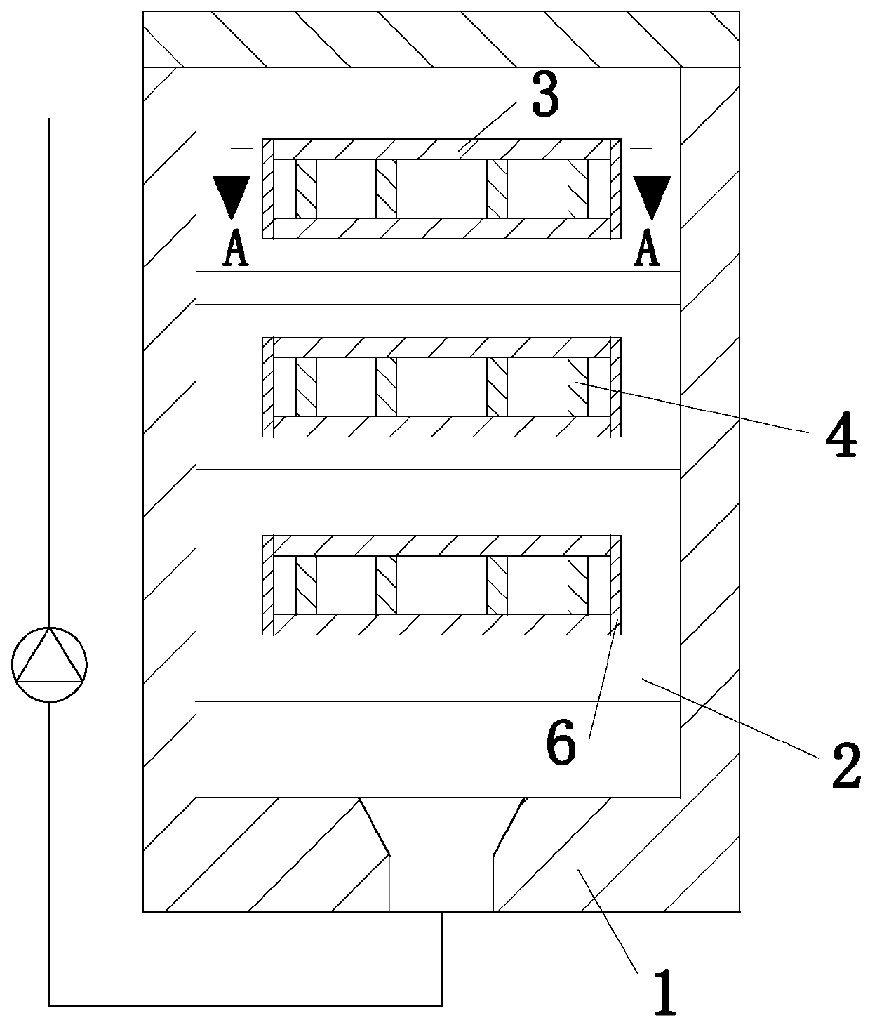
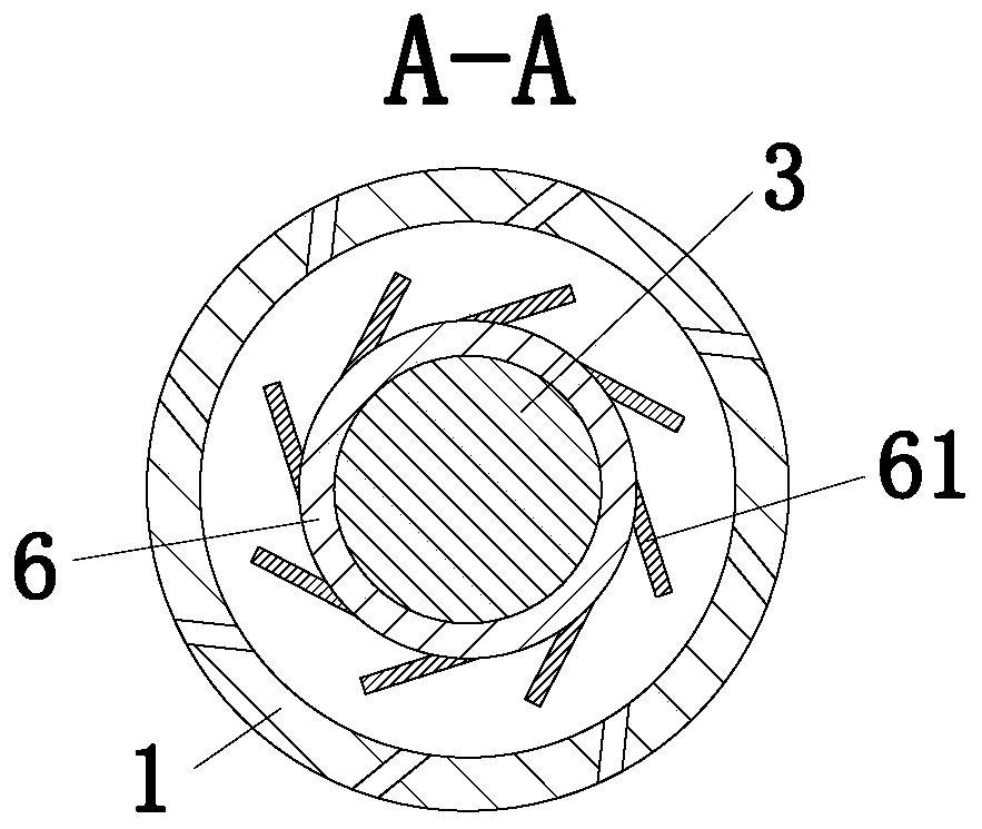
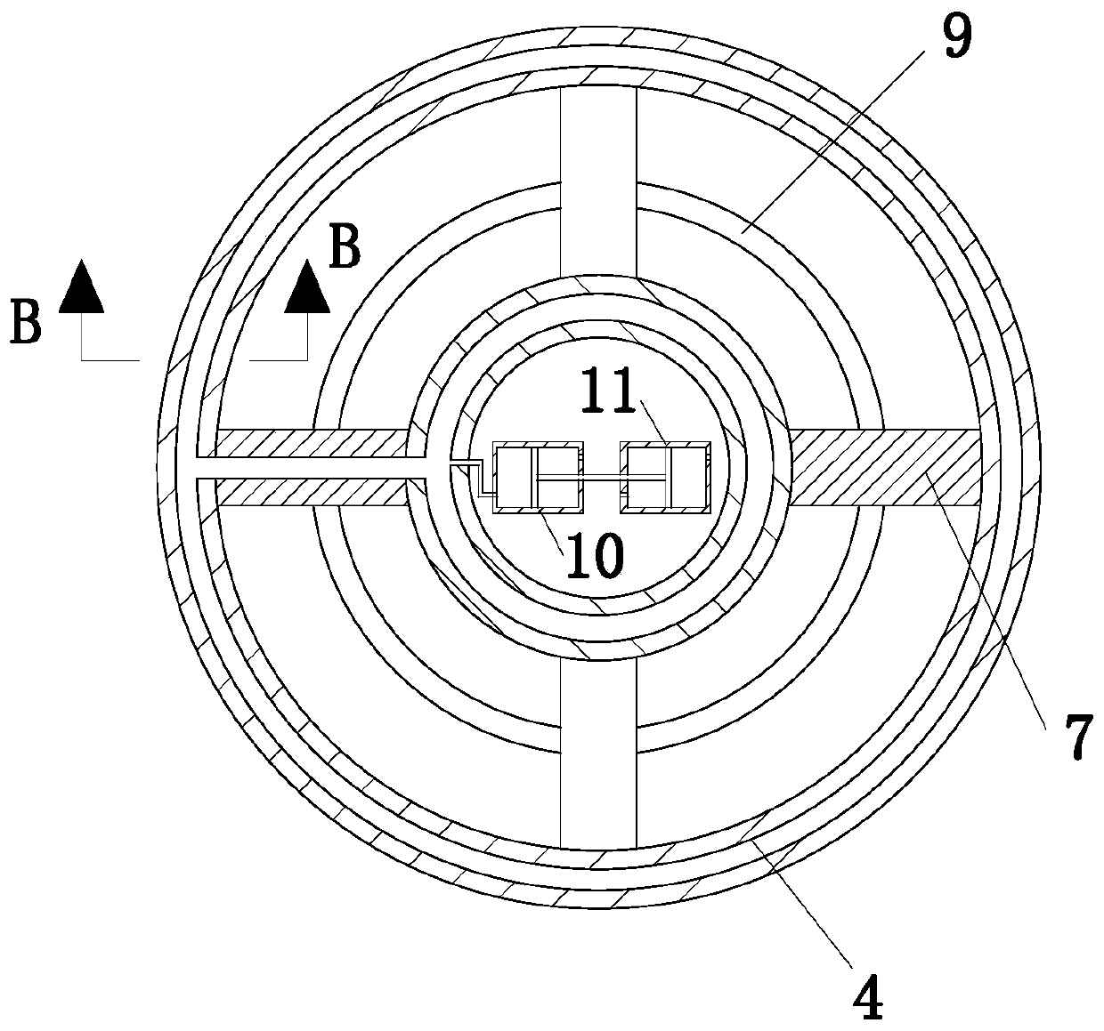
[0024] Such as Figure 1 to Figure 4 As shown, a semiconductor wafer electroplating device according to the present invention includes a reaction chamber 1, a magnetic ring 2, a wafer 3, a holder 4 and a permanent magnet 5, the reaction chamber 1 is cylindrical, and the wafer 3 The electroplating reaction is carried out in the reaction chamber 1. The upper part of the reaction chamber 1 is provided with a liquid inlet, and the bottom of the reaction chamber 1 is provided with a liquid outlet. The liquid outlet and the liquid inlet are connected by a pump and a hose to realize the electroplating solution. recycling; the magnetic ring 2 is horizontally fixed in the reaction chamber 1, and the magnetic ring 2 is evenly arranged in multiple layers in ...
PUM
 Abstract
Description
Claims
Application Information