Display panel, pixel circuit and driving method thereof

A technology of a pixel circuit and a driving method, which is applied in the field of display panels, can solve the problems of affecting the service life of the display panel, affecting the display effect, and reducing the brightness of the screen body, and achieves the effect of saving pins, facilitating hardware resources, and facilitating compensation.

Inactive Publication Date: 2019-04-12
KUNSHAN GO VISIONOX OPTO ELECTRONICS CO LTD
View PDF7 Cites 5 Cited by
  • Summary
  • Abstract
  • Description
  • Claims
  • Application Information

AI Technical Summary

Problems solved by technology

[0003] However, as time goes by, the efficiency of OLED (organic light-emitting diode, organic light-emitting diode) will also decline rapidly, which will lead to a gradual decrease in the brightness of the screen
Affect the display effect and affect the service life of the display panel

Method used


Image

  • Display panel, pixel circuit and driving method thereof
  • Display panel, pixel circuit and driving method thereof
  • Display panel, pixel circuit and driving method thereof

Examples


Embodiment Construction

[0016] The following will clearly and completely describe the technical solutions in the embodiments of the present application with reference to the drawings in the embodiments of the present application. Obviously, the described embodiments are only some of the embodiments of the present application, not all of them. Based on the embodiments in this application, all other embodiments obtained by persons of ordinary skill in the art without making creative efforts belong to the scope of protection of this application.

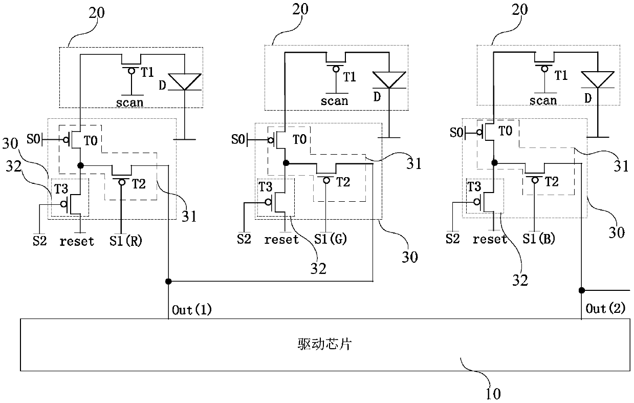
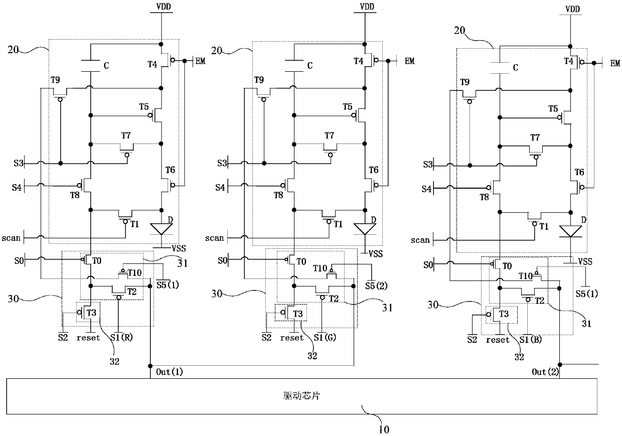
[0017] see figure 1 , figure 1 is a schematic diagram of the circuit structure of the pixel circuit in the first embodiment of the present application.

[0018] In this embodiment, the pixel circuit includes a driver chip 10 and several pixel circuit units 20 and several detection circuit units 30 connected to the driver chip 10 .

[0019] Each detection circuit unit 30 independently corresponds to a group of pixel circuit units 20 arranged along the first d...


PUM


Abstract

The application discloses a display panel, a pixel circuit and a driving method thereof. The pixel circuit includes a driving chip, and a plurality of pixel circuit units and a plurality of detectingcircuit units connected to the driving chip; the pixel circuit unit includes a first switching transistor and an electroluminescent element; each detecting circuit unit includes a selection circuit, and the selection circuit includes a second switching transistor and a connection switching transistor; a first access end of the second switching transistor is connected to an anode of the electroluminescent element in the pixel circuit unit through the connection switching transistor and the pixel circuit unit; the control end of the second switching transistor is connected to a first timing signal end; the second access end of the second switching transistor is connected to the driving chip; and at least two adjacent detecting circuit units are connected in a second direction through connection terminals, and the two adjacent detecting circuit units are connected to the same pin of the driving chip through the connection terminals. The application can facilitate the anode potential detection of a high pixel density display panel, and can improve the display effect of the display panel.

Description

technical field [0001] The invention relates to the field of display technology, in particular to a display panel, a pixel circuit and a driving method thereof. Background technique [0002] AMOLED (Active-matrix organic light-emitting diode, active-matrix organic light-emitting diode or active-matrix organic light-emitting diode) displays are widely used in mobile phones and TVs due to their advantages such as wide viewing angle and low power consumption. [0003] However, as time goes by, the efficiency of OLED (organic light-emitting diode, organic light-emitting diode) will also decline rapidly, which will lead to a gradual decrease in the brightness of the screen body. It affects the display effect and the service life of the display panel. Contents of the invention [0004] The main problem to be solved by the present application is to provide a display panel, a pixel circuit and a driving method thereof, which can improve the display effect of the display panel and...

Claims


Application Information

Patent Timeline
Patent Type & Authority Applications(China)
IPC IPC(8): G09G3/3225
CPCG09G3/3225
Inventor 范龙飞王龙彦朱晖韩珍珍胡思明吴剑龙张露
Owner KUNSHAN GO VISIONOX OPTO ELECTRONICS CO LTD
Why Eureka
Try Eureka