Array substrate, display panel, display device and driving method

A technology of array substrate and display panel, applied in the field of display panel and array substrate, can solve problems such as affecting the display effect of pixels

Active Publication Date: 2020-08-11
XIAMEN TIANMA MICRO ELECTRONICS
View PDF8 Cites 4 Cited by
  • Summary
  • Abstract
  • Description
  • Claims
  • Application Information

AI Technical Summary

Problems solved by technology

Use the scanning line to turn on the thin-film transistor in the pixel, and then provide data signals to each pixel in the row through the data line in turn. In...

Method used


Image

  • Array substrate, display panel, display device and driving method
  • Array substrate, display panel, display device and driving method
  • Array substrate, display panel, display device and driving method

Examples


Embodiment Construction

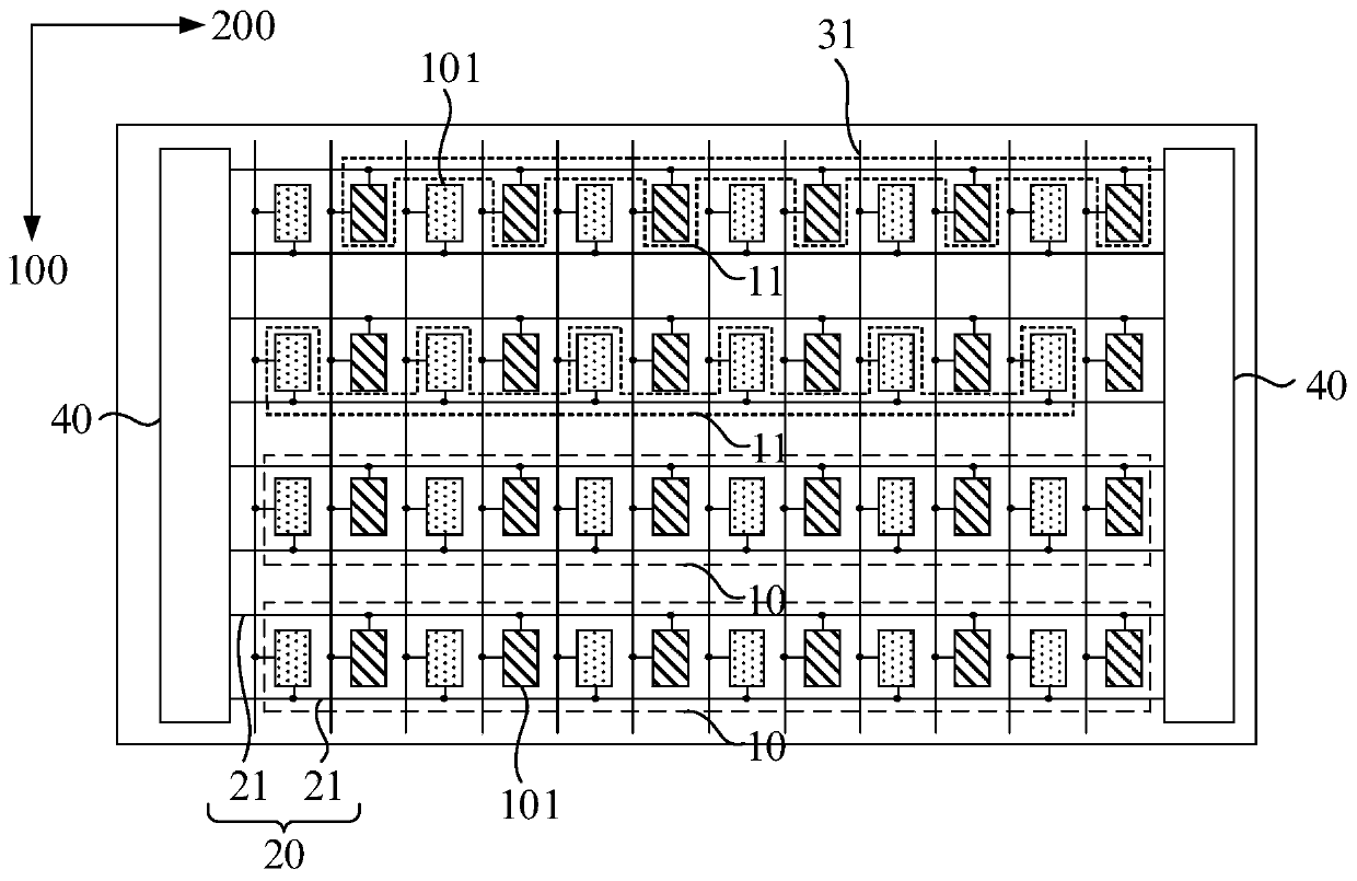
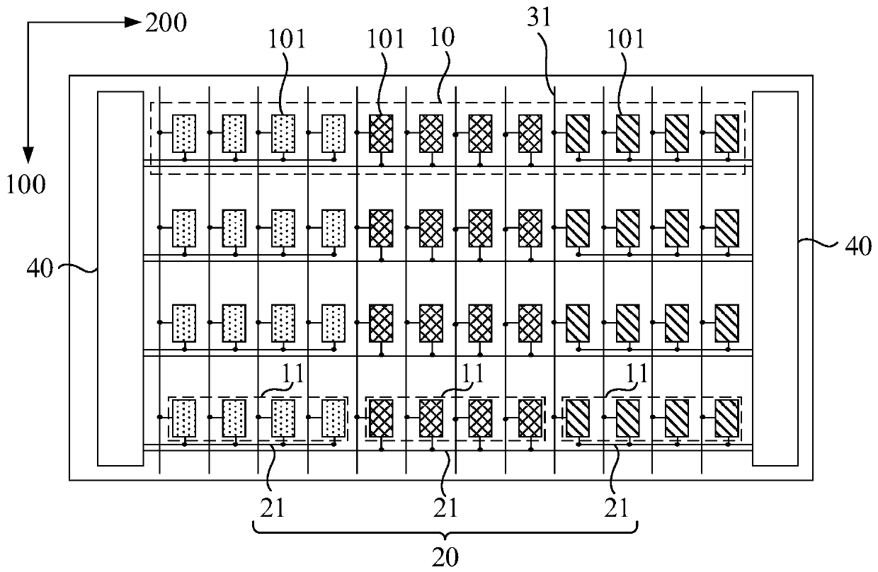
[0033] The present invention will be further described in detail below in conjunction with the accompanying drawings and embodiments. It should be understood that the specific embodiments described here are only used to explain the present invention, but not to limit the present invention. In addition, it should be noted that, for the convenience of description, only some structures related to the present invention are shown in the drawings but not all structures.

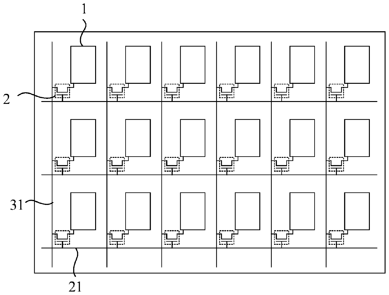
[0034] figure 1 It is a structural schematic diagram of the existing display panel, refer to figure 1 , the existing display panel is generally composed of many tiny pixels 1 arranged in a matrix, each pixel 1 is connected to a thin film transistor 2, and each thin film transistor 2 is connected to the scanning line 21 and the data line 31 to control the voltage of the pixel . Specifically, in the horizontal direction, the gate electrodes of all thin film transistors 2 are connected to the same scanning line 21;...


PUM


Abstract

The embodiment of the invention discloses an array substrate, a display panel, a display device and a driving method. The array substrate includes: a plurality of pixel circuit rows, each pixel circuit row including a plurality of pixel circuits; a plurality of scanning line group, each pixel circuit row comprising at least two pixel circuit groups, each scanning line group comprising at least twoscanning lines, the at least two pixel circuit groups and the at least two scanning lines in the corresponding scanning line groups being arranged in a one-to-one correspondence mode, and the pixel circuits in the same pixel circuit group being connected with the same scanning line. Different scanning line groups provide scanning signals for each pixel circuit row in sequence, and the scanning lines in the same scanning line group provide scanning signals for the pixel circuits in the corresponding pixel circuit rows at the same time. According to the embodiment of the invention, the problemof charging delay caused by excessive load of the existing display panel is solved. Each row of pixel circuits can be ensured to have sufficient charging duration, the pixel circuits can be opened accurately and timely, and the pixel charging delay is avoided.

Description

technical field [0001] Embodiments of the present invention relate to the field of display technologies, and in particular, to an array substrate, a display panel, a display device, and a driving method. Background technique [0002] With the continuous development of display technology, display devices such as liquid crystal panels and monitors are constantly developing in the direction of thinner and lighter, larger screen, lower power consumption and higher definition. [0003] For display panels with larger and larger sizes and higher resolutions, the number of pixels that need to be connected to the same row on each scanning line becomes larger. Use the scanning line to turn on the thin-film transistor in the pixel, and then provide data signals to each pixel in the row through the data line in turn. In the process of charging the pixel, the scanning signal provided on the scanning line will cause charging delay due to excessive load, affecting Pixel display effect. ...

Claims


Application Information

Patent Timeline
IPC IPC(8): G02F1/133G02F1/1362G09G3/3266G09G3/36
CPCG02F1/136286G02F1/13306G09G3/3266G09G3/3677G09G2310/0286G09G2320/0223G09G2310/0205H10K59/131H10K59/353
Inventor 吴常志孙莹许育民
Owner XIAMEN TIANMA MICRO ELECTRONICS
Why Eureka
Try Eureka