Display module, display device and manufacturing method of display module

A technology for display modules and manufacturing methods, applied to identification devices, parts of color TVs, parts of TV systems, etc., capable of solving dislocation of film layers, decline in screen ratio and aesthetics of OLED display panels, and impact on cameras Normal use and other problems, to achieve the effect of preventing interference

Active Publication Date: 2020-12-15
WUHAN CHINA STAR OPTOELECTRONICS SEMICON DISPLAY TECH CO LTD
View PDF6 Cites 11 Cited by
  • Summary
  • Abstract
  • Description
  • Claims
  • Application Information

AI Technical Summary

Problems solved by technology

[0004] The non-folding OLED display device can be used normally by using the above-mentioned production process; however, in the folding OLED display device, due to the difference in bending curvature of each film layer of the OLED display panel when bending, resulting in a gap between the film layers If there is a dislocation phenomenon, if the camera is combined into the round hole of the OLED display panel according to the above-mentioned production process, there is a risk of interference between the camera and the display panel, which will affect the normal use of the camera; if the above-mentioned risk of interference is to be avoided, the round hole of the OLED display panel The hole radius needs to be enlarged to a certain extent, resulting in a decline in the screen-to-body ratio and aesthetics of the OLED display panel

Method used


Image

  • Display module, display device and manufacturing method of display module
  • Display module, display device and manufacturing method of display module
  • Display module, display device and manufacturing method of display module

Examples


Embodiment Construction

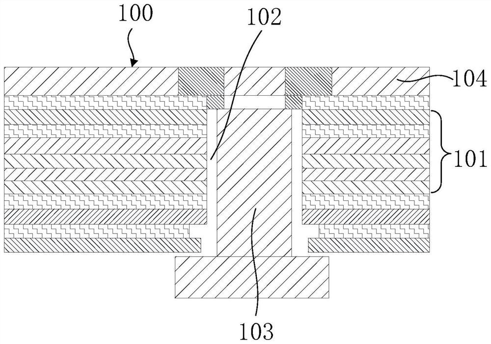
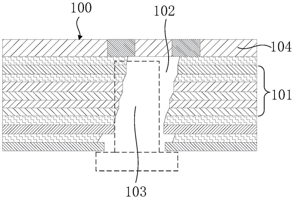
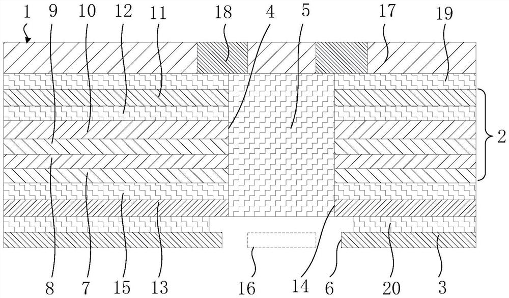
[0033] The technical solutions in the embodiments of the present application will be clearly and completely described below in conjunction with the drawings in the embodiments of the present application. Apparently, the described embodiments are only some of the embodiments of this application, not all of them. Based on the embodiments in this application, all other embodiments obtained by those skilled in the art without making creative efforts belong to the scope of protection of this application.

[0034] In the description of the present application, it should be understood that the terms "center", "longitudinal", "transverse", "length", "width", "thickness", "upper", "lower", "front", " Orientation indicated by rear, left, right, vertical, horizontal, top, bottom, inside, outside, clockwise, counterclockwise, etc. The positional relationship is based on the orientation or positional relationship shown in the drawings, which is only for the convenience of describing the a...


PUM


Abstract

The invention discloses a display module, a display device and a manufacturing method of the display module. The display module comprises a display panel and a metal supporting layer arranged on the back face of the display panel; a light-transmitting through hole is formed in the display panel, and an optical adhesive filling layer is arranged in the light-transmitting through hole; and the metalsupporting layer is provided with an accommodating through hole corresponding to and communicating with the light-transmitting through hole, and the accommodating through hole is used for arranging an optical sensor. According to the display module, the display device and the manufacturing method, the interference between the display panel and the optical sensor can be effectively prevented whenthe display module is folded, and meanwhile, the aperture of the light-transmitting through hole of the display panel is prevented from being enlarged.

Description

technical field [0001] The present application relates to the field of display technology, in particular to a display module, a display device and a method for manufacturing the display module. Background technique [0002] With the popularization of the concept of full screen, consumers have higher and higher requirements for the screen ratio of mobile phones. In order to increase the screen-to-body ratio, display technologies such as under-screen cameras, water drop screens, and openings in the screen have been gradually developed. At present, the under-display camera technology has not yet been mass-produced due to technical reasons, and water drop screens and in-screen perforated cameras have become the mainstream of display at this stage. [0003] The main production process of OLED (Organic Light-Emitting Diode, Organic Light-Emitting Diode) display device with in-screen aperture camera is as follows: use laser cutting to cut the OLED display panel into round holes ac...

Claims


Application Information

Patent Timeline
Patent Type & Authority Applications(China)
IPC IPC(8): G09F9/30G09F9/33H01L27/32H04N5/225
CPCG09F9/301G09F9/33H04N23/57H10K59/60H10K59/65H10K59/12H10K59/1201
Inventor 郑秉文
Owner WUHAN CHINA STAR OPTOELECTRONICS SEMICON DISPLAY TECH CO LTD
Why Eureka
Try Eureka