Chip and mainboard

A chip and bare chip technology, applied in the computer field, can solve the problems of occupying the area of ​​the printed circuit board, low integration of the main board, and occupying the space of other devices, so as to achieve small line width and length, high integration, and high data transmission speed. Effect

Pending Publication Date: 2021-02-19
HYGON INFORMATION TECH CO LTD
View PDF0 Cites 0 Cited by
  • Summary
  • Abstract
  • Description
  • Claims
  • Application Information

AI Technical Summary

Problems solved by technology

Due to the large size of the memory stick, and when the memory connector is set on the printed circuit board, it will occupy more area

Method used


Image

  • Chip and mainboard
  • Chip and mainboard
  • Chip and mainboard

Examples


Embodiment Construction

[0026] In order to make the purpose, technical solutions and advantages of the embodiments of the present invention clearer, the technical solutions in the embodiments of the present invention will be clearly and completely described below in conjunction with the drawings in the embodiments of the present invention. Obviously, the described embodiments It is only some embodiments of the present invention, but not all embodiments. Based on the embodiments of the present invention, all other embodiments obtained by persons of ordinary skill in the art without making creative efforts belong to the protection scope of the present invention.

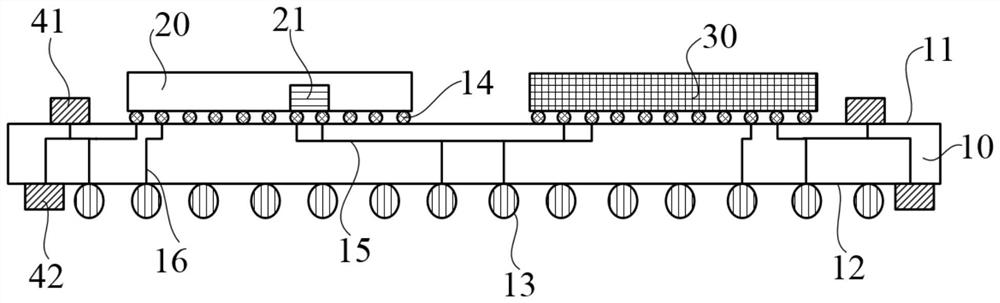
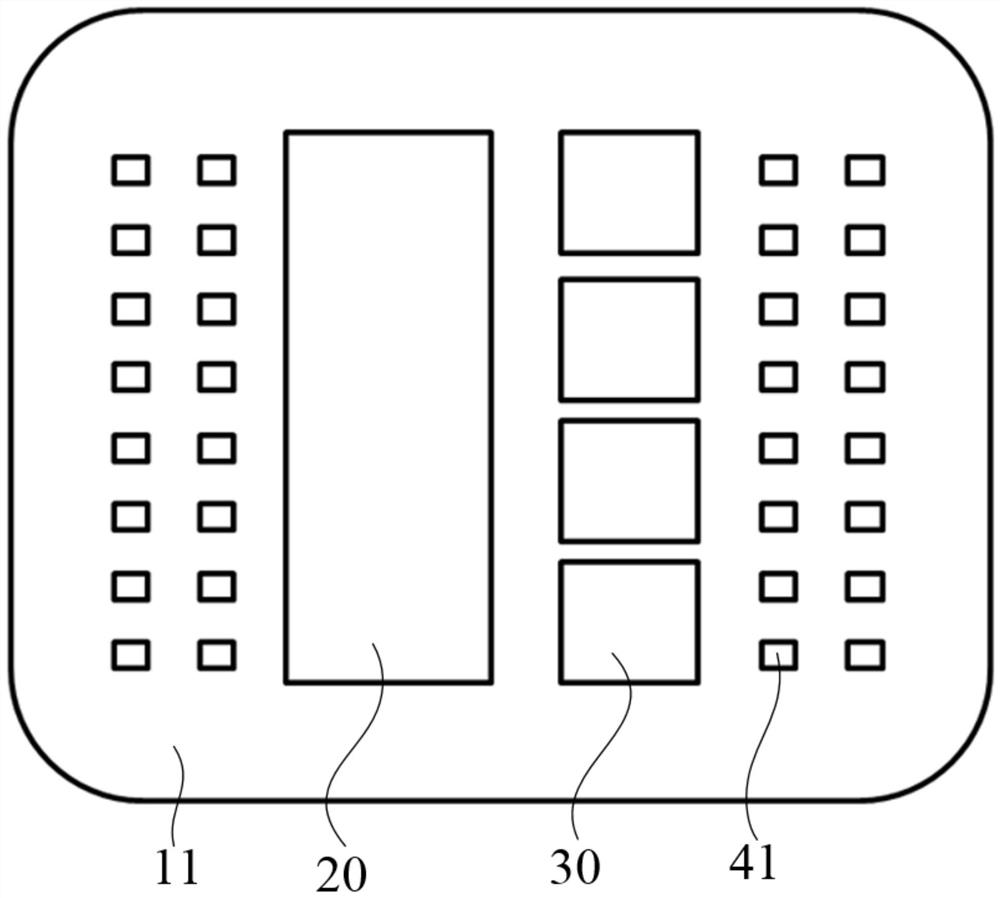
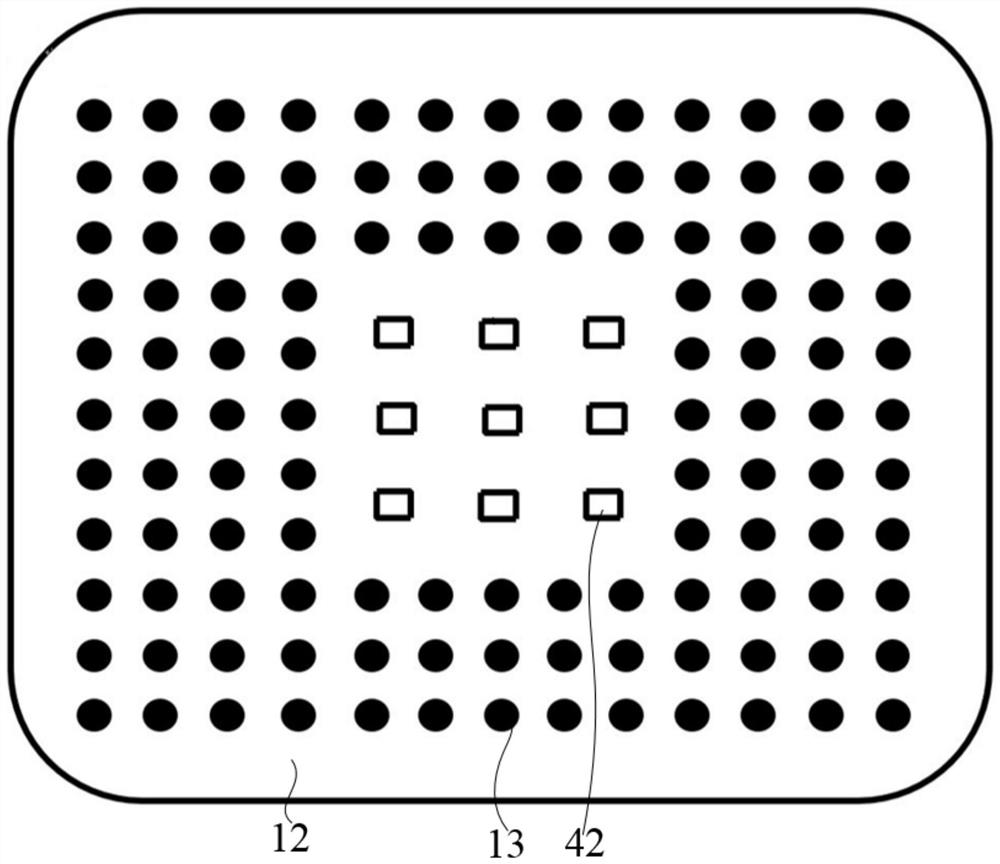
[0027] In order to facilitate the understanding of the chip provided by the embodiment of the present invention, the application scenarios of the chip provided by the embodiment of the present invention will be firstly described below. The chip is applied to computer equipment such as a server. The chip will be described in detail below in co...


PUM


Abstract

The invention provides a chip and a mainboard. The chip comprises a packaging substrate with a first surface and a second surface which are opposite to each other, and at least one memory bare chip arranged on the first surface of the packaging substrate. The first surface of the packaging substrate is provided with a central processing unit bare chip, and the central processing unit bare chip iselectrically connected with each memory bare chip in the at least one memory bare chip so as to write data into each memory bare chip or read data from each memory bare chip. The second surface of thepackaging substrate is provided with pins used for being electrically connected with the printed circuit board, and the central processor bare chip is further electrically connected with the pins onthe second surface. The central processing unit bare chip and the at least one memory bare chip are packaged on the packaging substrate, and each memory bare chip is electrically connected with the central processing unit bare chip, so that the central processing unit bare chip and the memory bare chip on the packaging substrate can work, the integration degree of the chip and the mainboard is improved. The area of a printed circuit board of a mainboard can be reduced, system design is simplified, and system reliability is improved.

Description

technical field [0001] The invention relates to the technical field of computers, in particular to a chip and a mainboard. Background technique [0002] With the development of computers at any time, device integration has gradually become a development trend. The connection mode between the central processing unit and the memory module of the motherboard in the prior art is as follows: a central processing unit and a plurality of memory connectors are arranged on the printed circuit board, and a memory bar is plugged into each memory connector. That is, all the memory on the motherboard is provided by the memory sticks on the printed circuit board. Since the size of the memory stick is relatively large, and when the memory connector is arranged on the printed circuit board, it will occupy more area of ​​the printed circuit board, thereby crowding out the installation space of other devices, so that the integration degree of the mainboard is low. Contents of the invention...

Claims


Application Information

Patent Timeline
IPC IPC(8): H01L23/498H01L25/18H05K1/11G06F1/16
CPCH01L25/18H01L23/49811H05K1/115G06F1/16H01L2224/16225H01L2924/15311H01L2924/15192H01L2924/15174
Inventor 林少芳杨晓君杜树安杨光林孟凡晓
Owner HYGON INFORMATION TECH CO LTD
Why Eureka
Try Eureka