Chip testing method and device, chip testing machine and storage medium

A technology for chip testing and storage media, applied in the fields of devices, chip testing methods, chip testing machines and storage media, can solve the problems of high chip power consumption, reduce test costs, reduce test power consumption, and reduce control difficulty Effect

Pending Publication Date: 2022-04-05
西安爱芯元智科技有限公司
View PDF0 Cites 2 Cited by
  • Summary
  • Abstract
  • Description
  • Claims
  • Application Information

AI Technical Summary

Problems solved by technology

[0004] In view of this, the purpose of the embodiments of the present application is to provide a chip testing method, device, chip testing machine and storage medium to improve the problem of high power consumption during chip testing in the prior art

Method used


Image

  • Chip testing method and device, chip testing machine and storage medium
  • Chip testing method and device, chip testing machine and storage medium
  • Chip testing method and device, chip testing machine and storage medium

Examples


Embodiment Construction

[0054] The following will clearly and completely describe the technical solutions in the embodiments of the present application with reference to the drawings in the embodiments of the present application. Apparently, the described embodiments are only some of the embodiments of the present application, but not all of them. Based on the embodiments of the embodiments of the present application, all other embodiments obtained by persons of ordinary skill in the art without making creative efforts belong to the scope of protection of the embodiments of the present application.

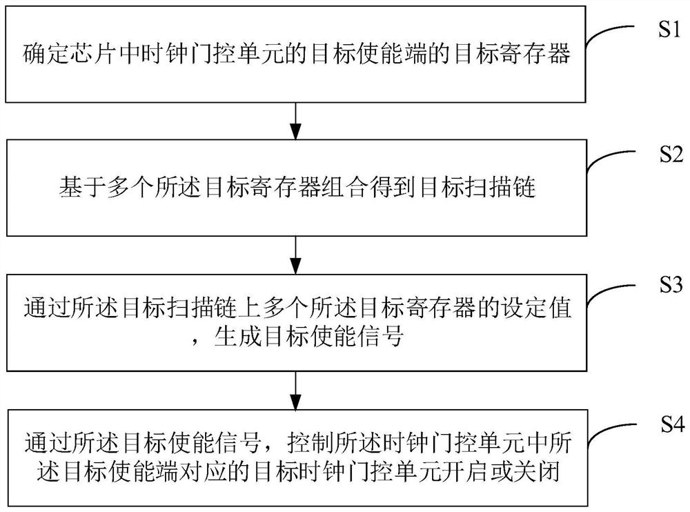
[0055] In the existing chip test, the test of the logic chip often uses the scan test technology, and the scan test is performed by connecting flip-flops in the chip in series to form a scan chain. In the existing scan test technology, the terminal of the integrated clock gating unit (Integrated Clock Gating, ICG) in the chip is connected to a unified chip port, which is usually multiplexed with the glob...


PUM


Abstract

The invention provides a chip testing method and device, a chip testing machine and a storage medium, and relates to the technical field of chip testing, and the method comprises the steps: determining a target register of a target enabling end of a clock gating unit in a chip; obtaining a target scan chain based on a plurality of target register combinations; generating a target enable signal through the set values of a plurality of target registers on the target scan chain; and controlling a target clock gating unit corresponding to a target enabling end in the clock gating units to be opened or closed through the target enabling signal. On the basis of generating the target scan chain, the clock gating unit can be controlled to be opened and closed in the chip scan test mode by controlling the value of the register, so that the control difficulty of the clock gating unit is reduced, the opening proportion of the clock gating unit is effectively controlled, the number of test vectors is reduced, the test coverage rate is improved, and the test efficiency is improved. Therefore, the test power consumption during the chip scanning test is reduced, and the test cost is reduced.

Description

technical field [0001] The present application relates to the technical field of chip testing, in particular, to a chip testing method, device, chip testing machine and storage medium. Background technique [0002] In chip design, clock gating technology is usually used to control the power consumption of the chip during normal operation. The clock gating technology uses an integrated clock gating unit (Integrated Clock Gating, ICG) to control the on and off of the flip-flop clock in the chip. When the flip-flop needs to work, the clock gating unit is turned on, and when the flip-flop does not need to work, the clock gating unit is turned off, thereby achieving the purpose of reducing chip power consumption. The clock gating unit generally has an E terminal and a TE terminal, the E terminal is a gating enabling terminal, and the TE terminal is a testing enabling terminal, respectively having two switch enabling signals E and TE. When the chip is working normally, the enabl...

Claims


Application Information

Patent Timeline
Patent Type & Authority Applications(China)
IPC IPC(8): G01R31/28
Inventor 孙军凯张柯孟祥刚蒋曦
Owner 西安爱芯元智科技有限公司
Why Eureka
Try Eureka