
Emitter coupled logic circuit having data heavy dnty function
A technology of emitter coupling and logic circuits, applied in logic circuits, logic circuits using specific components, logic circuits using semiconductor devices, etc., can solve data overload speed delay, affect ECL circuit data overload operation speed, design issues of complexity
- Summary
- Abstract
- Description
- Claims
- Application Information
AI Technical Summary
Problems solved by technology
Method used
Image

Examples
Embodiment Construction
[0011] The ECL circuit with data reloading of the present invention will be described in detail below with reference to the drawings.
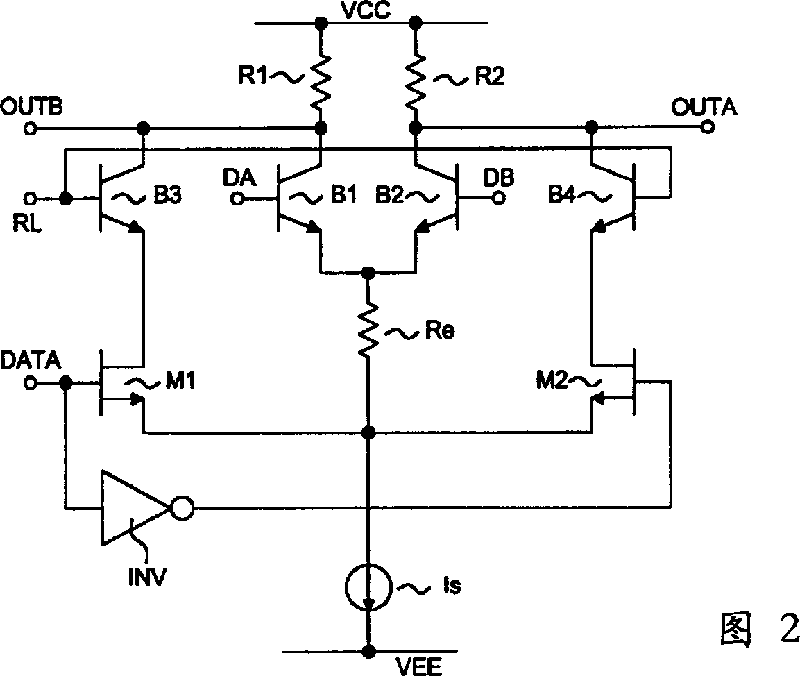
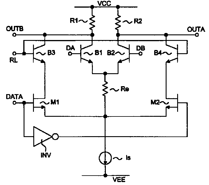
[0012] Fig. 2 is the ECL circuit with data reloading function of the present invention. As shown in the figure, the ECL circuit of the present invention includes a differential emitter coupled bipolar transistor pair B1, B2, a load resistor pair R1, R2, a pair of heavy load control bipolar transistors B3, B4, a connection A resistor Re at the emitter of the bipolar transistor pair B1, B2, a current source Is connected to the resistor Re, a pair of field effect transistors M1, M2 receiving heavy load data, and an inverter INV.
[0013] Collectors of the emitter-coupled bipolar transistor pair B1 and B2 are connected to a high operating voltage VCC through resistors R1 and R2 , and bases receive differential signals DA and DB respectively. The emitters of the emitter-coupled bipolar transistor pair B1, B2 are connected to a low operating voltag...
PUM
 Abstract
Description
Claims
Application Information