

Method of manufacturing laminated substrate
A manufacturing method and a technology of laminated substrates, applied in the field of manufacturing such electronic components and manufacturing such laminated substrates, can solve the problems of reduced grinding efficiency, increased risk, and the use of multi-layer wiring substrates, so as to improve grinding accuracy and simplify Grinding process, effect of preventing load concentration
- Summary
- Abstract
- Description
- Claims
- Application Information
AI Technical Summary
Problems solved by technology
Method used
Image

Examples
Embodiment Construction
[0026] Embodiments of the present invention will be described below with reference to the drawings.
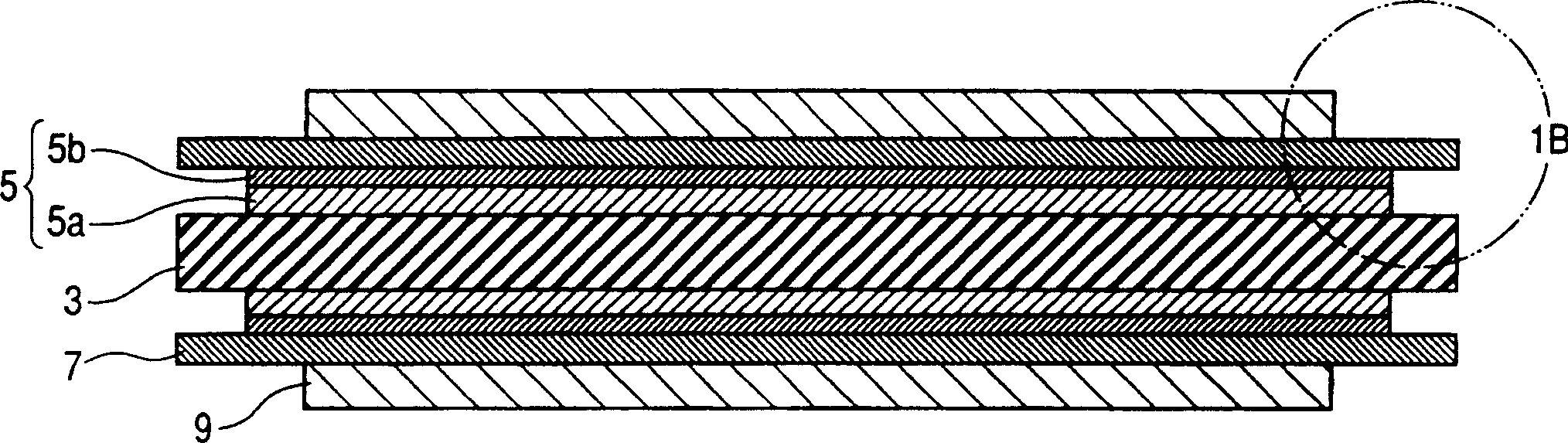
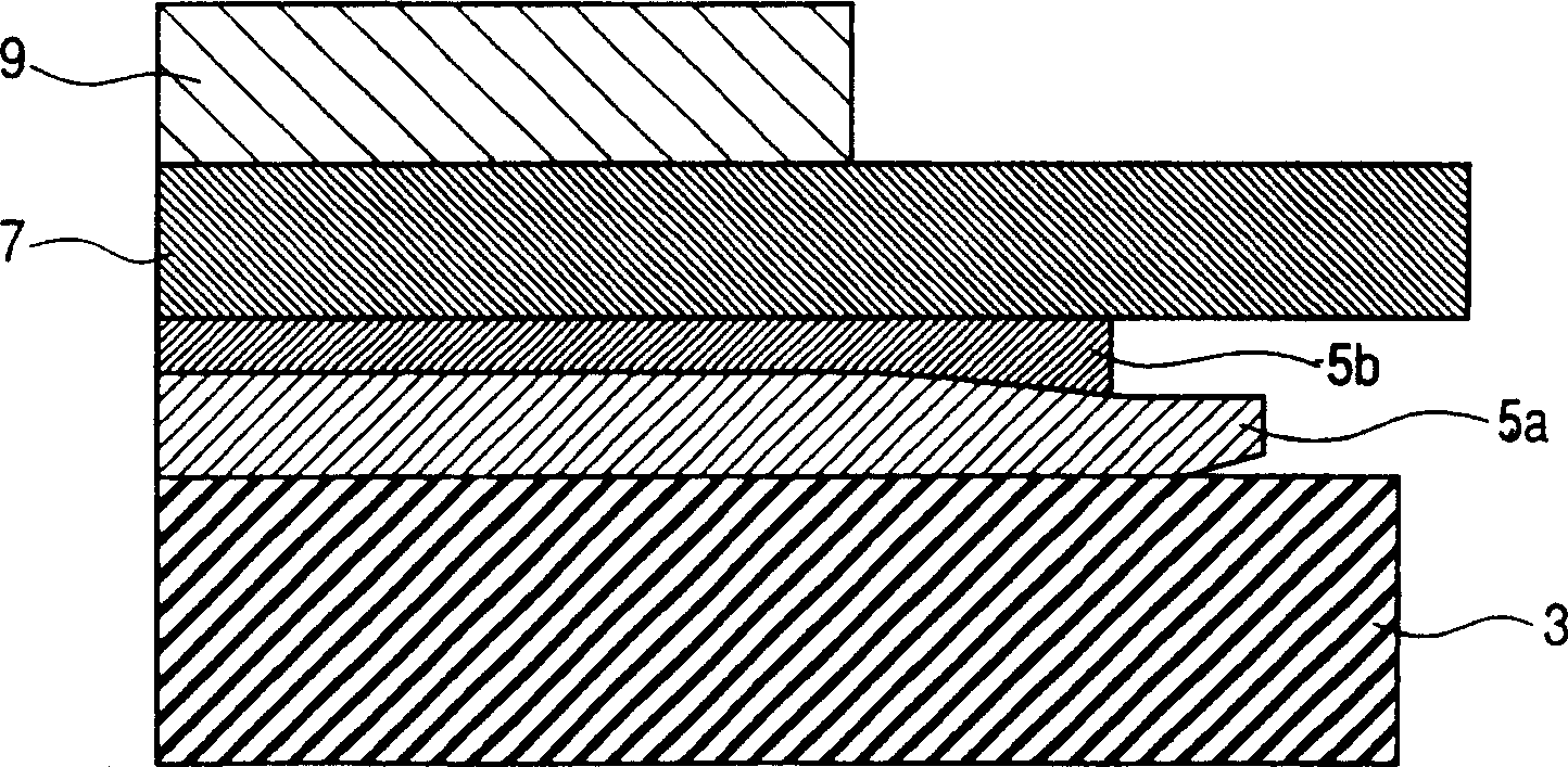
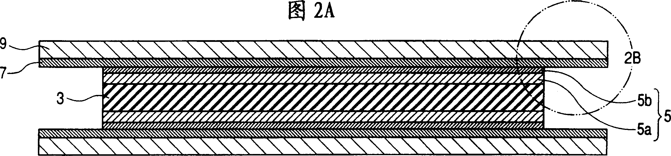
[0027] Figure 1A and 1B A buffer structure used in a pressing process according to an embodiment of the present invention is shown, in which a stacked state of a buffer member, a substrate, an RCC, and the like is shown in cross section. Figure 1A shows the overall structure, while Figure 1B is showing Figure 1A Magnified view of region 1B shown in . In the pressing process, the RCC 5, the stainless steel plate 7 and the cushioning member 9 are stacked in the stated order at the center of both sides of the thin plate-like substrate 3, and the press plate of the press (see Figure 4 ) are placed outside of them. The RCC 5 is formed by laminating a copper foil 5 b and a resin layer 5 a , and is oriented such that the resin layer 5 a side faces the substrate 3 . The substrate 3 is used as a core substrate, the RCC 5 is used as a metal foil with resin (ie, a metal foil to w...
PUM
 Abstract
Description
Claims
Application Information