Electronic circuit and data storage system

a technology of electronic circuits and data storage systems, applied in the field of electronic circuits, can solve the problems of not being able to modify individual components, not being able to modify the resistance value after manufacture, etc., and achieve the effect of fine control of the tuning or modification of the resistan

Active Publication Date: 2019-02-12
PRAGMATIC PRINTING
View PDF23 Cites 5 Cited by
  • Summary
  • Abstract
  • Description
  • Claims
  • Application Information

AI Technical Summary

Benefits of technology

[0006]This technique provides the advantage that the circuit can be modified or tuned after manufacturing the circuit in the first configuration by means of the irradiation, and so the resistance of the resisted element can be tuned, optimised, or otherwise adjusted after the initial part of the manufacturing and hence this can be used to modify the subsequent operation of the circuit. This tuning or modification can be used to correct or adjust resistance values resulting from the first part of the manufacturing process (i.e. which result in the circuit being in the first configuration), or the modification may be used to bring about a substantial and desired change in the operation of the circuit. This modification or tuning of the resistance value can also be achieved without requiring any direct physical contact to be made to the circuit. Also, the resistive element may be embedded, contained, encapsulated, or otherwise provided in a structure and the irradiation may still be able to achieve the desired change in resistance.
[0019]Thus, controlling the number of pulses of radiation used to irradiating the resistive element provides the advantage that the magnitude of the resistance change can be controlled, and in certain embodiments may be used to achieve a plurality of different magnitudes of change. Thus, fine control of the tuning or modification of the resistance can be achieved by means of selecting the number of pulses to be applied.

Problems solved by technology

Typically, no modification of that configuration (and in particular, no modification of individual components) is possible after manufacture.
The resistance of resisted elements in such circuits is typically fixed during manufacture, and those resistance values are not modifiable later on.

Method used


Image

  • Electronic circuit and data storage system
  • Electronic circuit and data storage system
  • Electronic circuit and data storage system

Examples


Embodiment Construction

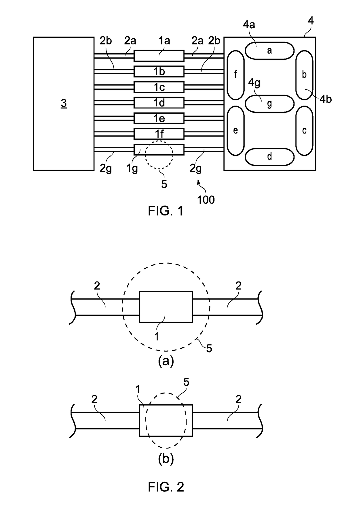
[0061]Referring now to FIG. 1, this is a schematic representation of an electronic circuit embodying the invention. The circuit 100 comprises a plurality of resistive elements 1a-1g, with each resistive element consisting of a thin, substantially planar rectangular layer of semiconductive / semiconductor material. The circuit further comprises drive circuitry 3 and a 7-segment display 4, comprising 7 individually controllable display segments 4a-4g. Each resistive element 1a-1g is coupled / connected to a respective one of the display segments 4a-4g by a conductive track 2a (which in this example is provided by a thin layer of metallic material, for example gold, silver, aluminium, copper, and each resistive element 1a-1g is also coupled to the drive circuitry 3 by means of a respective further conductive track 2a-2g. Each resistive element 1a-1g is arranged such that, before irradiation, its resistance is sufficiently high that, during operation of the circuit, its respective display s...


PUM

PropertyMeasurementUnit
thicknessaaaaaaaaaa
widthaaaaaaaaaa
sizeaaaaaaaaaa

Abstract

A method of manufacturing an electronic circuit comprises: providing an electronic circuit having a first configuration in which the circuit comprises a resistive element having a first resistance, and irradiating at least a part of the resistive element with electromagnetic radiation to change the resistance of the resistive element from the first resistance to a second resistance, the second resistance being lower than the first resistance. A method of storing data comprises: receiving a piece of data to be stored; determining a number according to the data; and irradiating at least part of a resistive element with that number of pulses of electromagnetic radiation to change a resistance of the resistive element from a first resistance to a second resistance, the second resistance being lower than the first resistance. A difference between the first resistance and the second resistance is dependent on the number. Corresponding circuits and data storage systems are disclosed.

Description

FIELD OF THE INVENTION[0001]The present invention relates to electronic circuits, methods of manufacturing electronic circuits, data storage systems, and methods of storing and reading data.BACKGROUND TO THE INVENTION[0002]Electronic circuits are, of course, extremely well-known. Typically, an electronic circuit is manufactured in a particular configuration and the subsequent operation of the circuit is determined by that configuration. Typically, no modification of that configuration (and in particular, no modification of individual components) is possible after manufacture. The resistance of resisted elements in such circuits is typically fixed during manufacture, and those resistance values are not modifiable later on.[0003]A wide variety of data storage and retrieval systems are also known, using a wide variety of techniques for storing data on a variety of storage media. There is an on-going need with such systems to find ways in which data may be stored securely, i.e. in a man...

Claims


Application Information

Patent Timeline
Patent Type & Authority Patents(United States)
IPC IPC(8): G02F1/13G11B9/04G11C13/00G11C11/56G11B11/12G11B11/08G11C13/04
CPCG11C13/047G11B9/04G11B11/08G11B11/12G11C13/044G11C13/0002G11C13/004G11C13/0007G11C13/0069G11C11/5685H01C17/242H10N70/20H10N70/257H10N70/823H10N70/8833G11C13/0004H10N70/883
Inventor PRICE, RICHARDRAMSDALE, CATHERINE
Owner PRAGMATIC PRINTING
Why Eureka
Try Eureka