Data transfer circuit and semiconductor integrated circuit equipped with data transfer circuit

a data transfer circuit and semiconductor technology, applied in the field of data transfer circuits, can solve the problems of difficult expansion of display function, display control circuits can only perform predetermined (designed) dma transfers,

Inactive Publication Date:
View PDF5 Cites 3 Cited by
  • Summary
  • Abstract
  • Description
  • Claims
  • Application Information

AI Technical Summary

Benefits of technology

[0014]In accordance with the embodiment of the invention described above, a first kind of data stored in one region of an external memory circuit can be transferred to another region of the external memory circuit based on a second kind of data that may be written and / rewritten by an external circuit. Accordingly, an expansion of the data transfer function can be readily made.

Problems solved by technology

However, according to the prior art technology, the CPU has to perform an interrupt processing (a processing to rewrite the image data in the frame memory) while temporarily stopping a processing being conducted at the time of generation of the interrupt.
However, this display control circuit can perform only predetermined (designed) DMA transfers.
Therefore, for example, when the number of icons to be blinked wants to be increased, there is a problem in that the hardware needs to be reconfigured, and thus it is not easy to expand the display function.

Method used


Image

  • Data transfer circuit and semiconductor integrated circuit equipped with data transfer circuit
  • Data transfer circuit and semiconductor integrated circuit equipped with data transfer circuit
  • Data transfer circuit and semiconductor integrated circuit equipped with data transfer circuit

Examples


Embodiment Construction

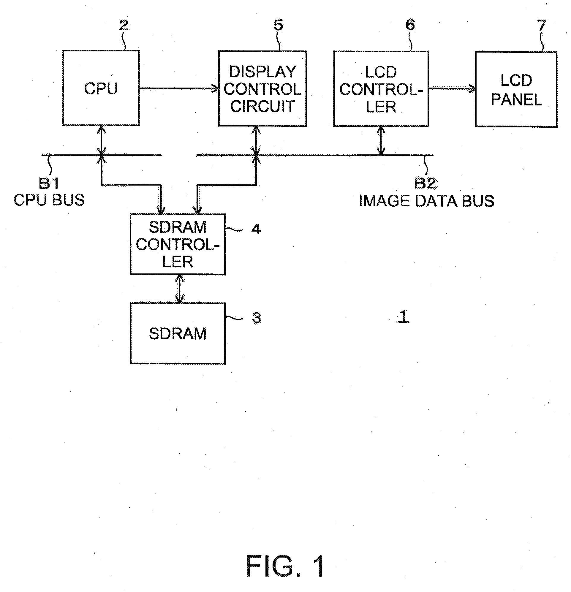
[0054]Preferred embodiments of the invention are described below with reference to the accompanying drawings. It is noted that the same components are appended with the same reference numerals, and their description is not repeated. FIG. 1 shows a schematic diagram of a system using a data transfer circuit in accordance with an embodiment of the invention. According to the present embodiment, the invention is applied to a display control circuit.

[0055]As shown in FIG. 1, the system 1 is equipped with a CPU 2, a SDRAM (synchronous DRAM) 3, a SDRAM controller 4, a display control circuit 5 in accordance with the present embodiment, a LCD controller 6, and a LCD panel 7.

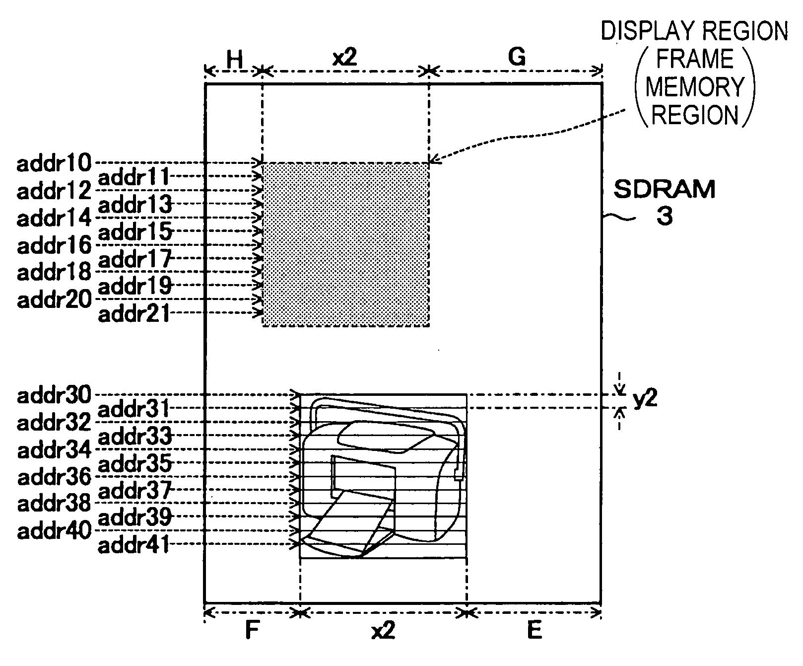
[0056]The SDRAM 3 is connected to and controlled by the SDRAM controller 4, has a portion that is used as a display region (frame memory region), and another portion that is used as a work area. The SDRAM controller 4 is connected to the CPU 2 through a CPU bus B1, and is connected to the display control circuit 5 and t...


PUM


Abstract

A data transfer circuit that transfers a first kind of data stored in an external memory circuit includes: an internal memory circuit that is capable of, by an external circuit, writing and/or rewriting a second kind of data including information for one region as a transfer source in the external memory circuit and another region as a transfer destination in the external memory circuit; a transfer circuit that transfer the first kind of data; and a control circuit that makes the transfer circuit transfer the first kind of data stored in the one region to the other region based on the second kind of data.

Description

[0001]The entire disclosure of Japanese Patent Application No. 2006-290091, filed Oct. 25, 2006 is expressly incorporated by reference herein.BACKGROUND[0002]1. Technical Field[0003]Several aspects of the invention relate to a data transfer circuit that transfers data stored in an external memory. Further, several aspects of the invention relate to a semiconductor integrated circuit equipped with such a data transfer circuit.[0004]2. Related Art[0005]Apparatuses that use a display device such as an LCD display device (for example, cellular phone devices, personal computers and the like) display blinking icons, animated icons and the like, for indicating that, for example, a battery has a few remaining capacity, an external device such as a printer, a hard disk device or the like is being accessed, etc.[0006]In general, image data for displaying an image is stored in a memory (frame memory). Addresses of a frame memory have one-to-one correspondence to positions (pixels) on a display...

Claims


Application Information

Patent Timeline
Patent Type & Authority Applications(United States)
IPC IPC(8): G06F13/372G09G5/39
CPCG09G3/3611G09G2310/04G09G5/391
Inventor MAKABE, TAKESHI
Why Eureka
Try Eureka