Optical device for scanning an information carrier

Inactive Publication Date: 2009-03-19
KONINKLIJKE PHILIPS ELECTRONICS NV
View PDF7 Cites 5 Cited by
  • Summary
  • Abstract
  • Description
  • Claims
  • Application Information

AI Technical Summary

Benefits of technology

[0007]By incorporating such an aberration optical element into the device; the performance of the device is improved. The aberration optical element provides a predetermined optical aberration to the radiation, to offset the aberration that would otherwise occur at the radiation spots e.g. in the image of the array optical element. This allows an increase in data density of the information carrier.

Problems solved by technology

However, due to the large amount of moving parts in the drives, known applications using this type of storage are not robust to shocks when performing read operations, considering the required stability of said moving parts during such operations.
As a consequence, optical storage cannot easily be used in applications that are subject to shocks, such as in portable devices.

Method used


Image

  • Optical device for scanning an information carrier
  • Optical device for scanning an information carrier
  • Optical device for scanning an information carrier

Examples


first embodiment

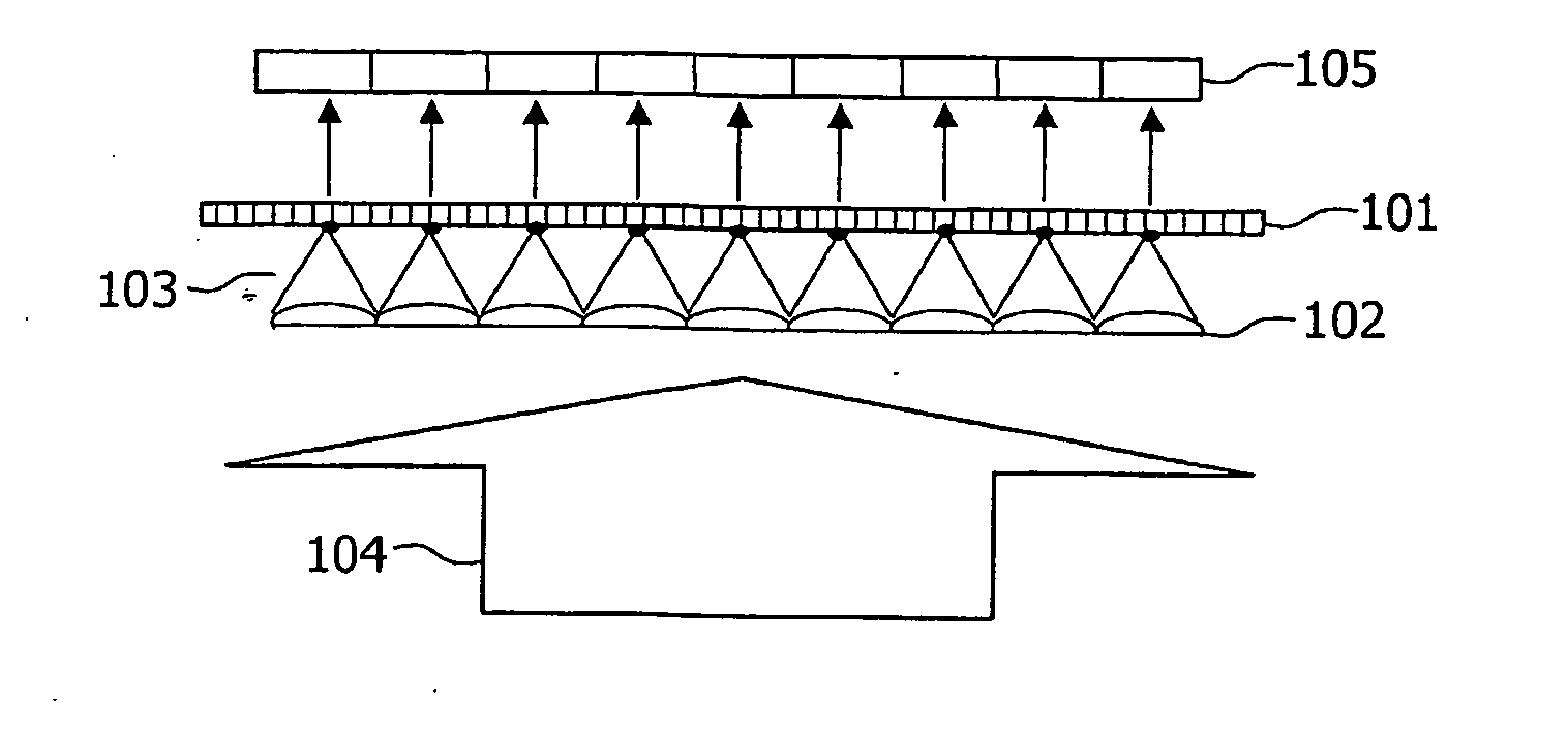
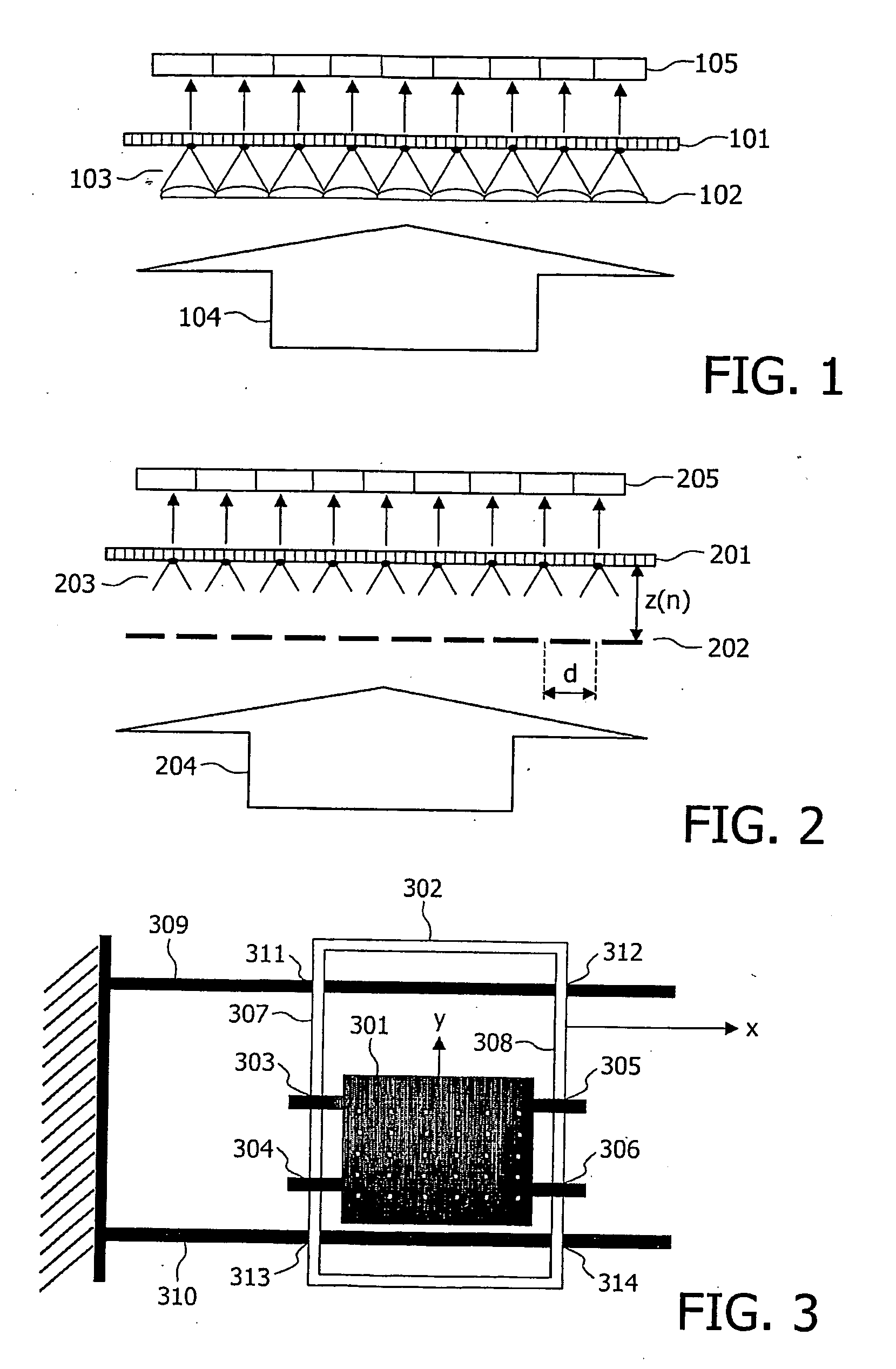
[0062]In a first embodiment depicted in FIG. 1, the system (i.e. the optical scanning device) for reading data stored on an information carrier 101 comprises an optical element 102 for generating an array of light spots 103 from an input light beam 104, said array of light spots 103 being intended to scan the information carrier 101.

[0063]The optical element 102 corresponds to a two-dimensional array of micro-lenses at the input of which the coherent input light beam 104 is applied. The array of micro-lenses 102 is placed parallel and distant from the information carrier 101 so that light spots are focussed on the information carrier. The numerical aperture and quality of the micro-lenses determines the size of the light spots. For example, a two-dimensional array of micro-lenses 102 having a numerical aperture which equals 0.3 can be used. The input light beam 104 can be realized by a waveguide (not represented) for expanding an input laser beam, or by a two-dimensional array of co...

second embodiment

[0067]In a second embodiment depicted in FIG. 2, the system for reading data stored on an information carrier 201 comprises an optical element 202 for generating an array of light spots 203 from an input light beam 204, said array of light spots 203 being intended to scan the information carrier 201.

[0068]The optical element 202 corresponds to a two-dimensional array of apertures at the input of which the coherent input light beam 204 is applied. The apertures correspond for example to circular holes having a diameter of 1 μm or smaller. The input light beam 204 can be realized by a waveguide (not represented) for expanding an input laser beam, or by a two-dimensional array of coupled micro lasers.

[0069]The light spots are applied on transparent or non-transparent areas of the information carrier 201. If a light spot is applied on a non-transparent area, no output light beam is generated in response by the information carrier. If a light spot is applied on a transparent area, an out...


PUM


Abstract

An optical scanning device for scanning an information carrier. The device includes an array optical element arranged to generate an array of radiation spots from an incident radiation beam, for the scanning of the information carrier. The device further includes an aberration optical element arranged to apply a predetermined optical aberration to the radiation for correction of optical aberration in the radiation spots.

Description

FIELD OF THE INVENTION[0001]The present invention relates to an optical scanning device for scanning an information carrier using an array of radiation spots, an optical element for use in such a device, and a scanning method. The invention may be used in the field of optical data storage.BACKGROUND OF THE INVENTION[0002]Optical storage is widely used for content distribution, for example in storage systems based on the CD (Compact Disc) and DVD (Digital Versatile Disc) standards. Optical storage has a big advantage over hard-disc and solid-state storage in that the information carriers are easy and cheap to replicate.[0003]However, due to the large amount of moving parts in the drives, known applications using this type of storage are not robust to shocks when performing read operations, considering the required stability of said moving parts during such operations. As a consequence, optical storage cannot easily be used in applications that are subject to shocks, such as in portab...

Claims


Application Information

Patent Timeline
IPC IPC(8): G11B7/00G11B7/12G11B7/135G11B7/14
CPCG11B7/12G11B7/1374G11B7/14G11B7/13922G11B7/1381G11B7/1392G02B26/10
Inventor HENDRIKS, ROBERT FRANS MARIASTALLINGA, SJOERDHENDRIKS, BERNARDUS HENDRIKUS WILHELMUS
Owner KONINKLIJKE PHILIPS ELECTRONICS NV
Why Eureka
Try Eureka