Glass Substrate of Flat Panel Display and Display Integrated Circuit Chip

a flat panel display and integrated circuit chip technology, applied in the field of flat panel displays, can solve the problems of waste of chip area and achieve the effect of increasing the miniaturization of glass substrates and excessive length of ic chips

Inactive Publication Date: 2009-05-14
AU OPTRONICS CORP
View PDF2 Cites 4 Cited by
  • Summary
  • Abstract
  • Description
  • Claims
  • Application Information

AI Technical Summary

Benefits of technology

[0007]The present invention relates to a glass substrate of flat panel display, can achieve an increased miniaturization.
[0008]The present invention further relates to a display integrated circuit chip, can achieve efficient utilization of chip area.
[0016]In the above-mentioned embodiments of the present invention, since output terminals of each IC chip are arranged at least two of the multiple sides thereof, facilitating the efficient utilization and miniaturization of the IC chip, and the drawback of a waste of chip area resulting from excessive length for the IC chip in the prior art is overcome. When the IC chip is applied to a glass substrate of flat display panel, an increased miniaturization for the glass substrate can be achieved.

Problems solved by technology

Each of the gate driver IC chips 12 and source driver IC chips 14 includes multiple sides and all of the output terminals thereof only are arranged at one long side of the multiple sides, resulting in an excessive length for the IC chip and a waste of chip area, and a region occupied by each IC chip on the glass substrate 10 is relatively large correspondingly.

Method used


Image

  • Glass Substrate of Flat Panel Display and Display Integrated Circuit Chip
  • Glass Substrate of Flat Panel Display and Display Integrated Circuit Chip
  • Glass Substrate of Flat Panel Display and Display Integrated Circuit Chip

Examples


Embodiment Construction

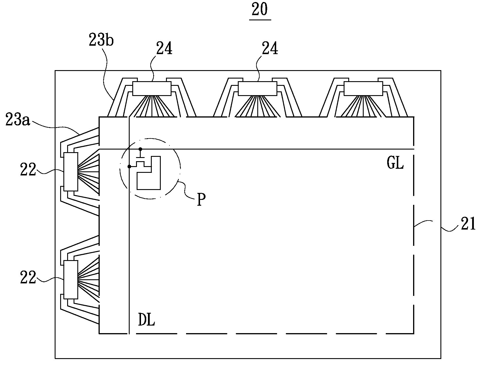
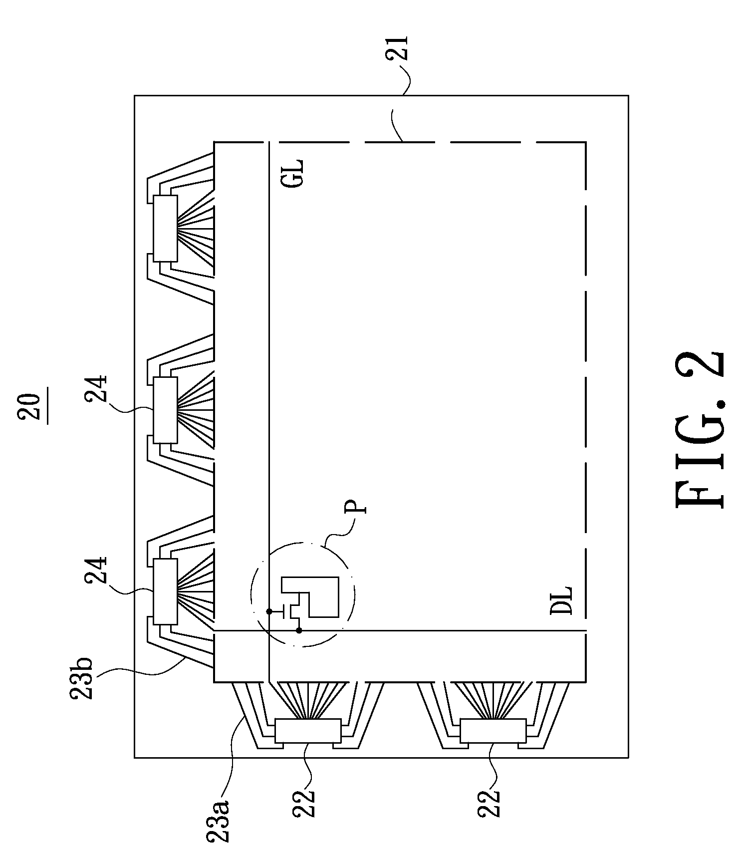
[0028]Referring to FIG. 2, a glass substrate 20 of flat panel display in accordance with an embodiment of the present invention is provided. The glass substrate 20 is adapted for disposing a plurality of gate driver IC chips 22 and a plurality of source driver IC chips 24 thereon. The glass substrate 20 includes a display area 21 (as denoted by the dashed rectangle in FIG. 2), a plurality of first conductive wires 23a and a plurality of second conductive wires 23b. The display area 21 have a plurality of display elements P, a plurality of gate lines GL and a plurality of data lines DL formed therein. In this embodiment, FIG. 2 only shows one display element P, one gate line GL and one data line DL for the purpose of illustration, the display element P is electrically coupled to the gate line GL and the data line DL. The first conductive wires 23a are electrically coupled between four sides of the gate driver IC chips 22 and the display area 21, so as to transmit gate control signals...


PUM


Abstract

An exemplary glass substrate of flat panel display is adapted for an integrated circuit (IC) chip. The IC chip has two opposite long sides and two opposite short sides. The glass substrate includes a display area and a plurality of conductive wires. The display area has a plurality of display elements formed therein. The conductive wires are electrically coupled to the IC chip and the display area, to transmit a signal provided from the IC chip to the display area. The IC chip includes a plurality of output terminals arranged at the long sides and electrically coupled to the respective conductive wires. The present invention also provides a display IC chip for receiving and outputting a first color signal, a second color signal and a third color signal.

Description

CROSS-REFERENCE TO RELATED APPLICATIONS[0001]This application is based upon and claims the benefit of priority from the prior Taiwanese Patent Application No. 097143431, filed Nov. 10, 2008, the entire contents of which are incorporated herein by reference.BACKGROUND[0002]1. Technical Field[0003]The present invention generally relates to the field of flat panel display and, particularly, to a glass substrate of flat panel display and a display integrated circuit (IC) chip.[0004]2. Description of the Related Art[0005]Flat panel displays such as a liquid crystal display (LCD) and a plasma display have the advantages of high image quality, small size, light weight and a broad application range, and thus are widely applied on consumer electronic products such as a mobile phone, a notebook computer, a desktop display and a television, and have gradually replaced the traditional cathode ray tube (CRT) displays as the main trend in the display industry.[0006]Referring to FIG. 1, a conventi...

Claims


Application Information

Patent Timeline
Patent Type & Authority Applications(United States)
IPC IPC(8): H01L23/498
CPCG09G2300/0426G02F1/13452G09G3/3674G09G3/3685
Inventor HSU, SHENG-KAIYANG, CHIH-HSIANGHSIEH, MENG-TING
Owner AU OPTRONICS CORP
Why Eureka
Try Eureka