

Pixel circuit and display device
a display device and pixel technology, applied in the field of pixel circuits and display devices, can solve the problems of deterioration of display quality, insufficient contrast, and the average potential in each frame period also decreases, and achieves the effect of low power consumption
- Summary
- Abstract
- Description
- Claims
- Application Information
AI Technical Summary
Benefits of technology
Problems solved by technology
Method used
Image

Examples
first embodiment
[0080]In the first embodiment, configurations of a display device of the present invention (to be simply referred to as a “display device” hereinafter) and a pixel circuit of the present invention (to be simply referred to as a “pixel circuit” hereinafter) will be described below.
[0081]
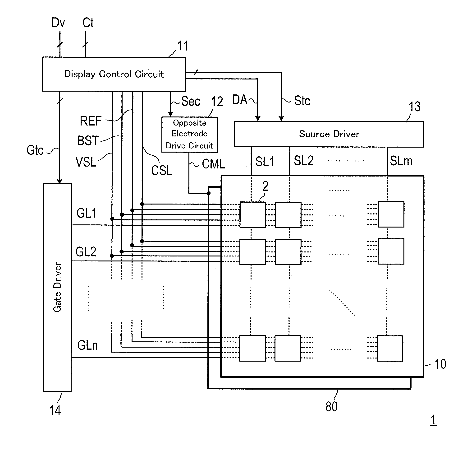
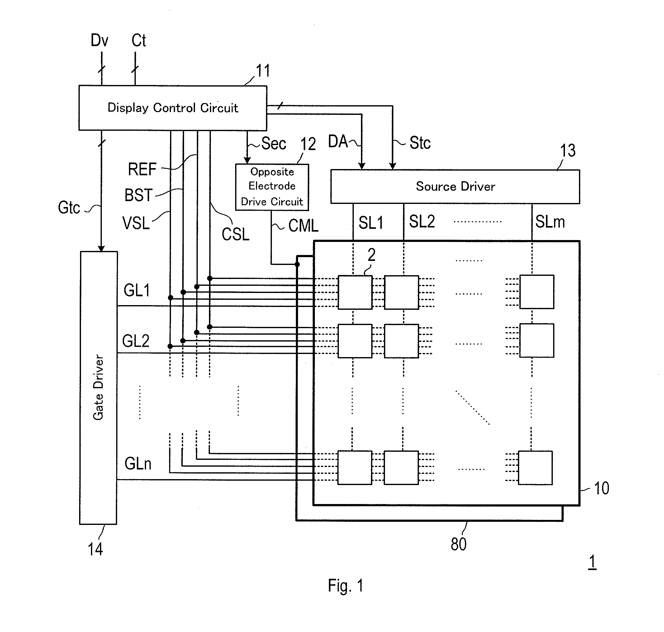
[0082]FIG. 1 shows a schematic configuration of a display device 1. The display device 1 includes an active matrix substrate 10, a counter electrode 80, a display control circuit 11, a counter electrode drive circuit 12, a source driver 13, a gate driver 14, and various signal lines (will be described later). On the active matrix substrate 10, a plurality of pixel circuits 2 are arranged in row and column directions to form a pixel circuit array.
[0083]In FIG. 1, to avoid the drawings from being complex, the pixel circuits 2 are displayed to be blocked. In order to clarify that the various signal lines are formed on the active matrix substrate 10, for descriptive convenience, the active matrix substrat...
second embodiment
[0141]In the second embodiment, self-refresh actions performed by the pixel circuits of the first to third types will be described below with reference to the drawings.
[0142]The self-refresh action is an action in an always-on display mode, and is an action in which the first switch circuit 22, the second switch circuit 23, and the control circuit 24 are operated by a predetermined sequence in the plurality of pixel circuits 2 to recover a potentials of a pixel electrode 20 (or a potential of the internal node N1) to a potential of a gradation level written by an immediately previous writing action, and the potentials are recovered for the pixel circuits having all the gradation levels at the same time in a lump in units of gradation levels. The self-refresh action is an action being unique to the present invention and performed by the pixel circuits 2A to 2E. The self-refresh action can achieve a very low power consumption in comparison with an “external refresh action” that perfor...
third embodiment
[0230]In the third embodiment, a case in which a self-refresh action is executed by a voltage applying method different from that in the second embodiment will be described with reference to the accompanying drawings. The self-refresh action of the embodiment, as in the second embodiment, is divided into a refresh step S1 and a standby step S2.
[0231]In the second embodiment, only the internal node N1 in the case H (high-voltage writing) is refreshed in the phase P1, and only the internal node N1 in the case M (intermediate-voltage writing) is refreshed in the phase P2. In the step S1, pulse voltage application to the boost line BST needs to be performed in each of the phase P1 and the phase P2.
[0232]In contrast to this, in the embodiment, as will be described later, only the internal node N1 in the case M (intermediate-voltage writing) is refreshed in the phase P1, and only the internal node N1 in the case H (high-voltage writing) is refreshed in the phase P2. In the step S1, a high...
PUM
 Abstract
Description
Claims
Application Information