Flash memory device and electronic device employing thereof

a flash memory and electronic device technology, applied in the field of flash memory devices, can solve the problems of increasing the probability of a bit error, deteriorating the character of a nand flash memory, etc., and achieve the effect of efficient data processing

Inactive Publication Date: 2013-08-29
SAMSUNG ELECTRONICS CO LTD
View PDF6 Cites 25 Cited by
  • Summary
  • Abstract
  • Description
  • Claims
  • Application Information

AI Technical Summary

Benefits of technology

[0010]An aspect of the present invention is to provide a NAND flash memory device for efficiently processing data that is larger than a page size of a data block and for processing data that is smaller than the page size of the data block.

Problems solved by technology

However, as the construction of the NAND flash produces more miniaturized flash devices, the characteristic of a NAND flash memory deteriorate because of several reasons including a narrow gap between cells, the occurrence of interference, and an increase of the probability of a bit error.

Method used


Image

  • Flash memory device and electronic device employing thereof
  • Flash memory device and electronic device employing thereof
  • Flash memory device and electronic device employing thereof

Examples


Embodiment Construction

[0029]Preferred exemplary embodiments of the present invention will be described herein below with reference to the accompanying drawings. In the following description, well-known functions or constructions may not be described in detail when their inclusion would obscure the appreciation of the invention by the person of ordinary skill in the art with unnecessary detail regarding well-known functions or constructions. In addition, terms described below, which are defined considering functions in the present invention, can be different depending on user and operator's intention or practice. Therefore, the terms should be defined on the basis of the disclosure throughout this specification.

[0030]Below, the present invention describes a flash memory device for efficiently supporting an array of a small page size.

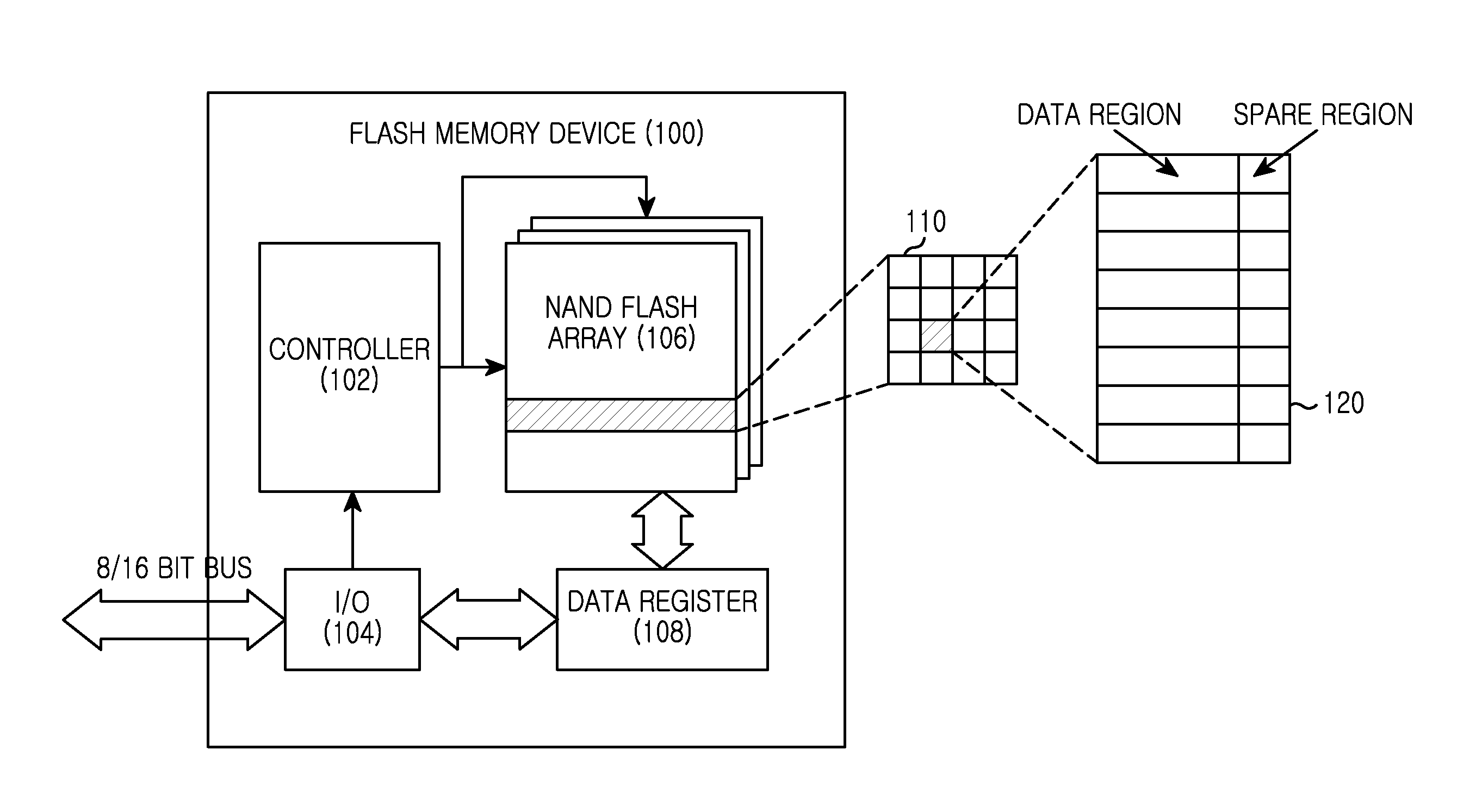
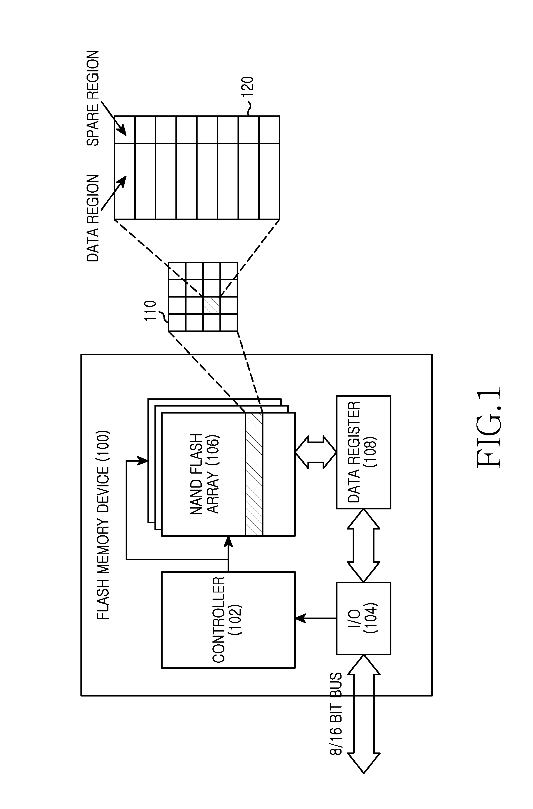
[0031]FIG. 1 illustrates a flash memory device according to an exemplary embodiment of the present invention.

[0032]Referring now to FIG. 1, the flash memory device 100 prefera...


PUM


Abstract

A flash memory device and an electronic device employing thereof are provided for efficiently processing data that is larger than a page size of a data block and for processing data that is smaller than the page size of the data block. The flash memory device preferably includes a plurality of flash arrays therein and the plurality of flash arrays is divided into partitions depending on at least two or more page sizes, thereby advantageously improving the performance of random write.

Description

CLAIM OF PRIORITY[0001]This application claims the benefit of priority under 35 U.S.C. §119(a) from a Korean Patent Application filed in the Korean Intellectual Property Office on Feb. 23, 2012 and assigned Ser. No. 10-2012-0018431, the contents of which are herein incorporated by reference in its entirety.BACKGROUND OF THE INVENTION[0002]1. Field of the Invention[0003]The present invention generally relates to a flash memory device. More particularly, the present invention relates to a flash memory device that can efficiently support, for example, an array of a small page size in an electronic device.[0004]2. Description of the Related Art[0005]As smart phones and other types of mobile devices become more and more widespread worldwide, the demand for a mobile storage system has continued to increase. To meet this increased demand, recently, a flash memory based storage system is being in the spotlight.[0006]More particularly, a Not AND (NAND) flash device, a non-volatile memory, is...

Claims


Application Information

Patent Timeline
Patent Type & Authority Applications(United States)
IPC IPC(8): G06F12/02
CPCG06F2212/7208G06F12/0246G06F12/02G06F12/06
Inventor LEE, JUN-WOO
Owner SAMSUNG ELECTRONICS CO LTD
Why Eureka
Try Eureka