

Multilayered optical film, manufacturing method thereof, and display device
Active Publication Date: 2013-11-14
SAMSUNG ELECTRONICS CO LTD +1
View PDF8 Cites 26 Cited by
- Summary
- Abstract
- Description
- Claims
- Application Information
AI Technical Summary
Benefits of technology
[0012]In an embodiment, the first phase retardation layer may have a short-wavelength dispersion value in a range from about 1.00 to about 1.05, the second phase retardation layer may have a short-wavelength dispersion value in a range from about 1.00 to
Problems solved by technology
However, conventional optical compensation films may have strong dependency on the wavelength of incident light such that the film may
Method used
View moreImage
Smart ImageViewing Examples

Examples
 PUM
| Property | Measurement | Unit |
|---|---|---|
| Angle | aaaaa | aaaaa |
| Angle | aaaaa | aaaaa |
| Angle | aaaaa | aaaaa |
Abstract
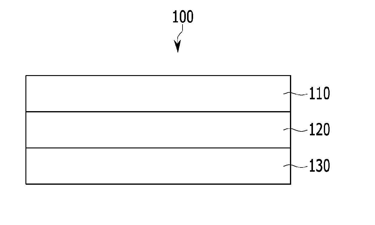
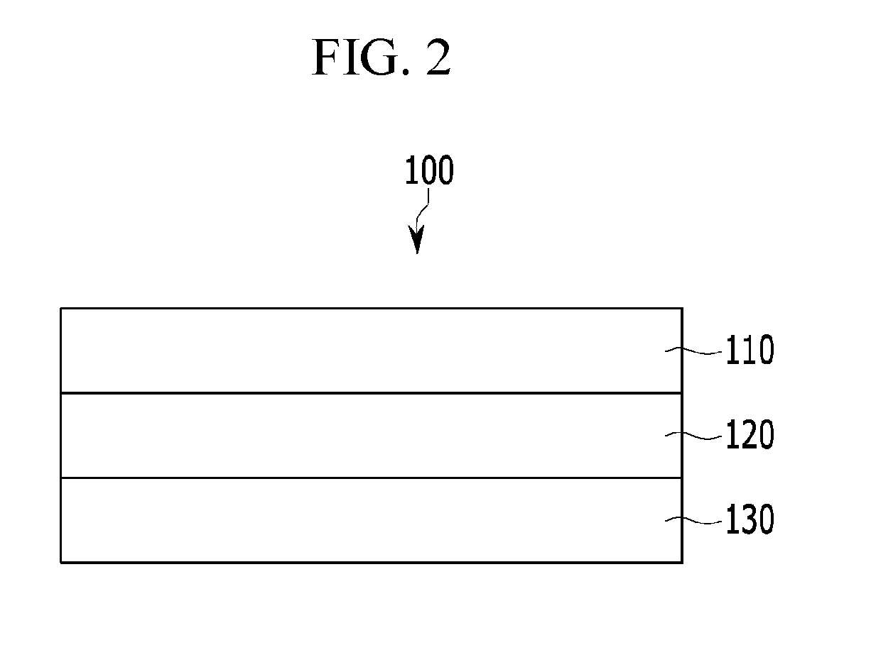
An optical film includes: a polarization layer; a first phase retardation layer having an optic axis at an angle in a range from about 17 degrees to about 27 degrees or from about −27 degrees to about −17 degrees with respect to a transmission axis of the polarization layer; and a second phase retardation layer having an optic axis at an angle in a range from about 85 degrees to about 95 degrees with respect to the transmission axis of the polarization layer. The polarization layer, the first phase retardation layer, and the second phase retardation layer are deposited in sequence, the first phase retardation layer is a half-wave plate, the second phase retardation layer is a quarter-wave plate, and out-of-plane retardation values of the first phase retardation layer and the second phase retardation layer for incident light having the standard wavelength have opposite signs.
Description
CROSS-REFERENCE TO RELATED APPLICATIONS[0001]This application claims priority to Korean Patent Application No. 10-2012-0049647 filed on May 10, 2012 and Korean Patent Application No. 10-2013-0052872 filed on May 10, 2013, and all the benefits accruing therefrom under 35 U.S.C. §119, the content of which in its entirety is herein incorporated by reference.BACKGROUND[0002](a) Field[0003]Provided is an optical film, and in particular, a multilayered optical film, a manufacturing method of the optical film, and a display device including the optical film.[0004](b) Description of the Related Art[0005]Flat panel displays may be classified into an emitting display device that emits light by itself and a non-emitting display device that uses separate light sources. An optical compensation film such as a phase difference film may be used for improving image quality of the flat panel displays.[0006]In the emitting display device, for example, an organic light emitting display, visibility and ...
Claims
Login to View More Application Information
Patent Timeline
 IPC IPC(8): G02B5/30B29D11/00
CPCG02B5/3083B29D11/00788B29C55/045B29D11/0073B29K2023/38B29K2029/04B29K2995/0034B32B37/12B32B38/0008B32B2037/1276B32B2038/0028B32B2307/40G02B5/3025
InventorIN, KYU YEOLKIM, HEE KYUNGJUNG, WON CHEOLKIM, HYUNG JUNOH, KYOUNG AHLEE, MOON YEONJUNG, MYUNG SUP
OwnerSAMSUNG ELECTRONICS CO LTD