Single-layer optical point-to-point network

Inactive Publication Date: 2014-05-01
ORACLE INT CORP
View PDF22 Cites 0 Cited by
  • Summary
  • Abstract
  • Description
  • Claims
  • Application Information

AI Technical Summary

Benefits of technology

The patent describes a way to route optical waves in a way that minimizes the distance between the sources and the circuits. This reduces the likelihood of signal loss and interference between the circuits. The techniques also allow for simultaneous communication among the integrated circuits.

Problems solved by technology

Using existing inter-layer optical couplers, the four inter-layer optical couplers shown in FIG. 1 will result in an optical loss of 12 dB.
This may limit the energy efficiency of the WDM optical links and the optical network, which can increase the power consumption of the MCM.

Method used


Image

  • Single-layer optical point-to-point network
  • Single-layer optical point-to-point network
  • Single-layer optical point-to-point network

Examples


Embodiment Construction

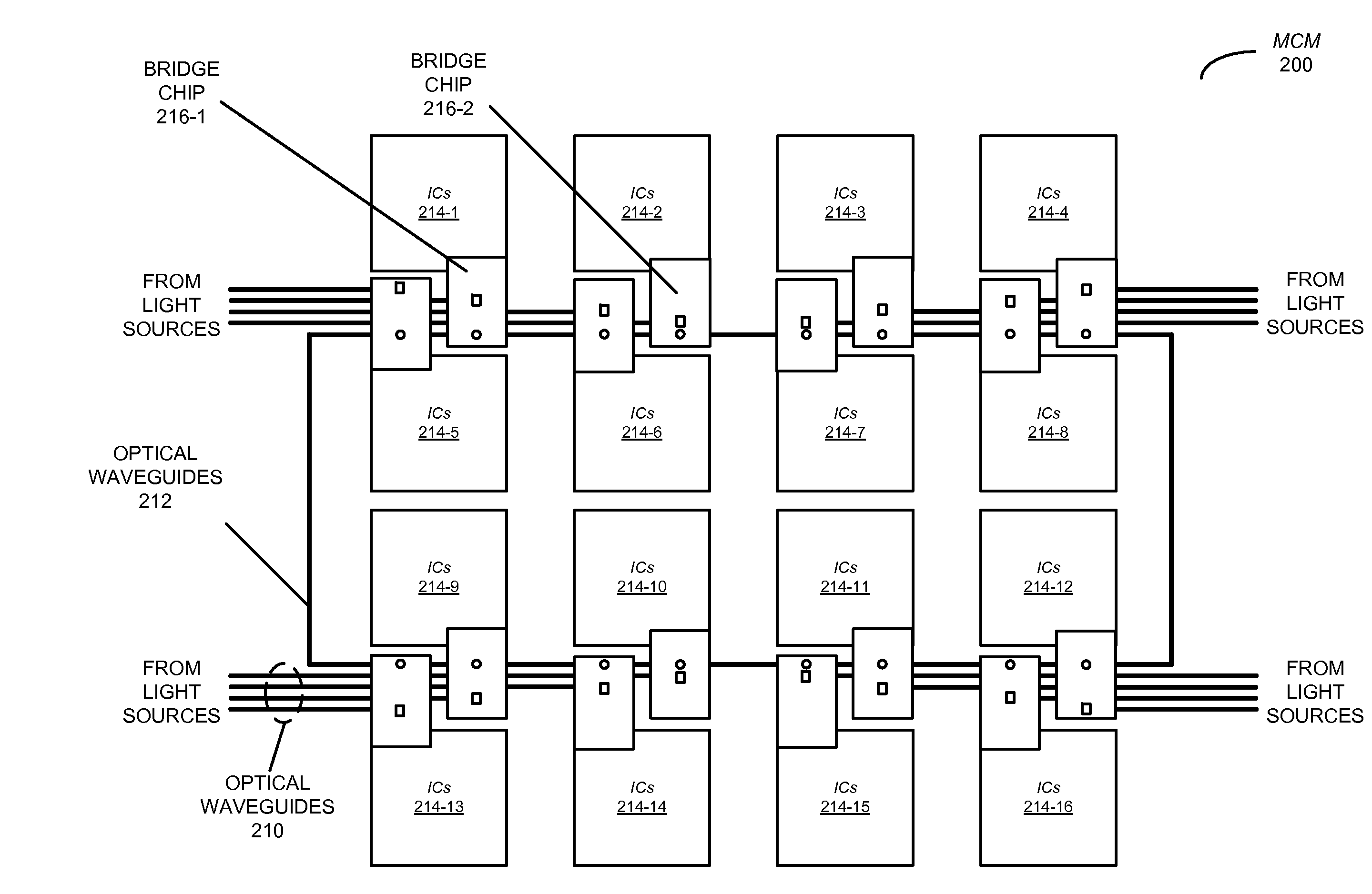
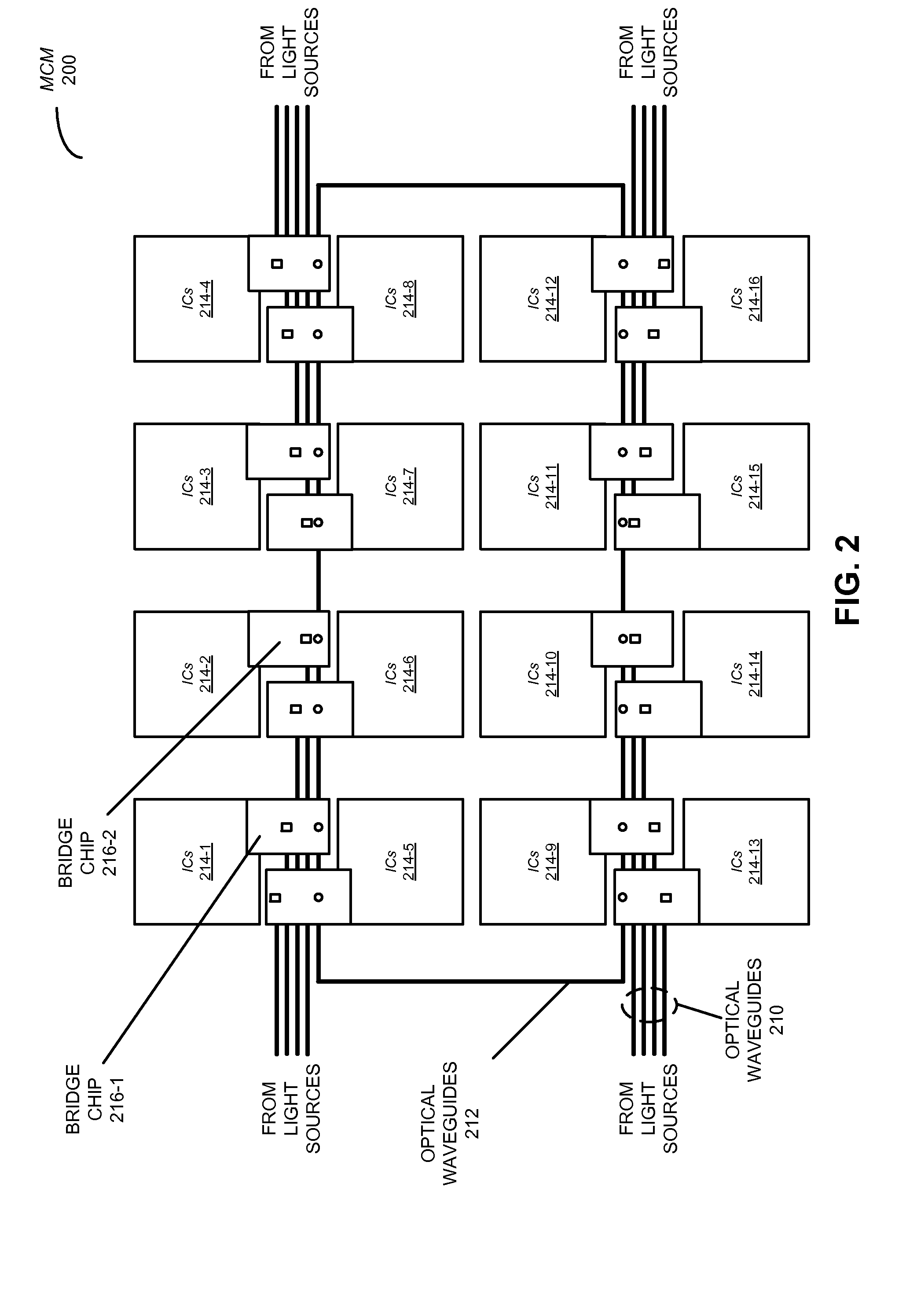
[0030]Embodiments of a multi-chip module (MCM), a system that includes the MCM, and a method for communicating information in the MCM are described. In this MCM, first and second optical waveguides convey optical signals among integrated circuits (which are sometimes referred to as ‘chips’). The first and second optical waveguides may be implemented in a first layer or plane on a substrate. Moreover, bridge chips in a second plane may be used to couple the optical signals between the first or second optical waveguides and the integrated circuits. By using a single layer for optical routing, the MCM may provide a point-to-point network among the integrated circuits without optical-waveguide crossing.

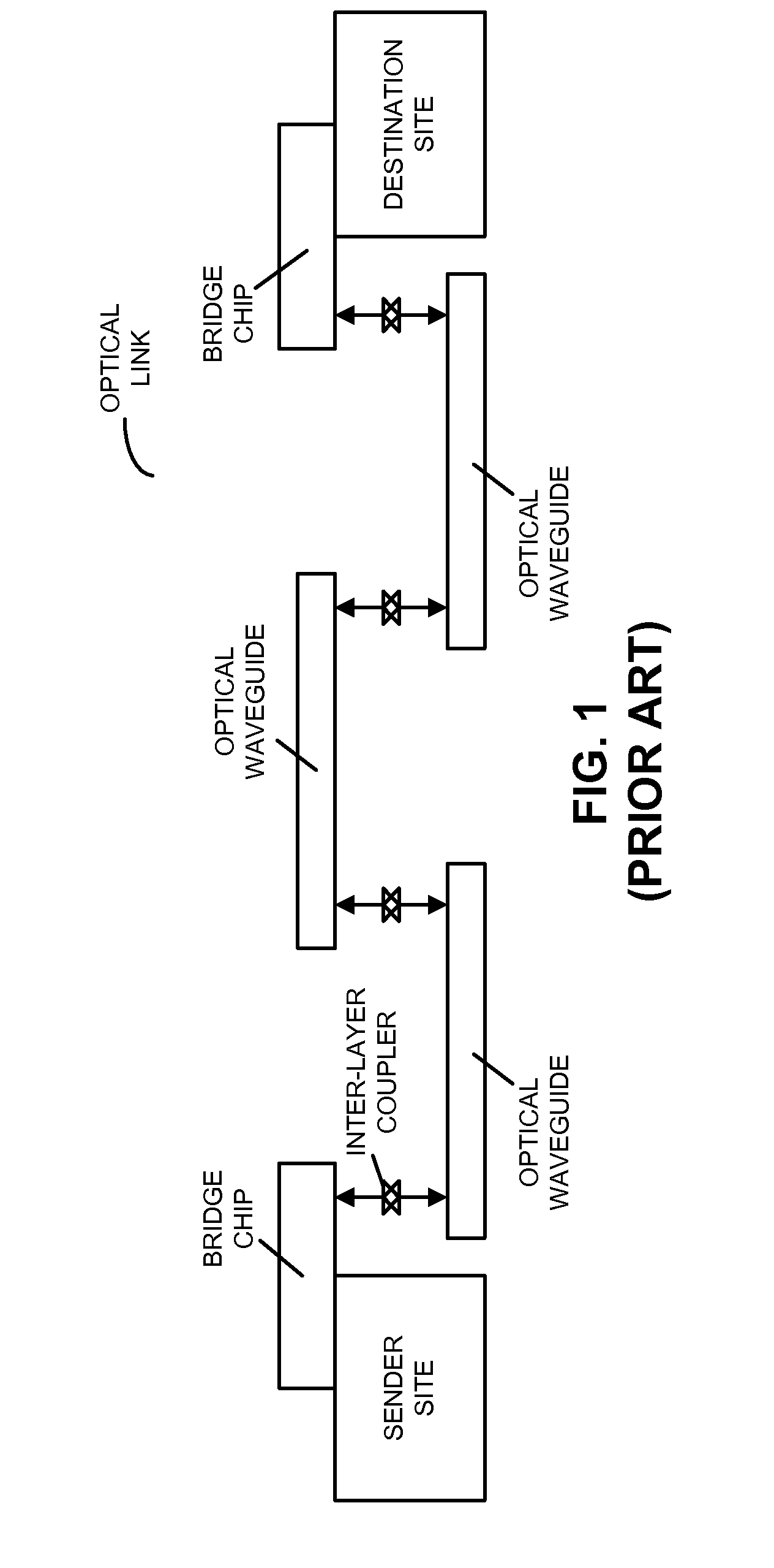
[0031]Using this communication technique, optical links among the integrated circuits in the MCM may use fewer inter-layer optical couplers, thereby reducing optical losses. For example, an optical link between a given pair of integrated circuits may include two inter-layer optical couple...


PUM


Abstract

In a multi-chip module (MCM), first and second optical waveguides convey optical signals among integrated circuits. The first and second optical waveguides may be implemented in a first layer or plane on a substrate. Moreover, bridge chips in a second plane may be used to couple the optical signals between the first or second optical waveguides and the integrated circuits. By using a single layer for optical routing, the MCM may provide a point-to-point network among the integrated circuits without optical-waveguide crossing.

Description

CROSS-REFERENCE[0001]This application is related to U.S. application Ser. No. 13 / 648,140, entitled “Opportunistic Bandwidth Stealing in Optical Networks,” by Arslan Zulfiqar, Pranay Koka and Herbert D. Schwetman, Attorney Docket Number ORA13-0240, filed on Oct. 9, 2012, the contents of which are herein incorporated by reference.GOVERNMENT LICENSE RIGHTS[0002]This invention was made with Government support under Agreement No. HR0011-08-9-0001 awarded by DARPA. The Government has certain rights in the invention.BACKGROUND[0003]1. Field[0004]The present disclosure generally relates to optical networks. More specifically, the present disclosure relates to a multi-chip module (MCM) that includes integrated circuits that communicate via an optical network.[0005]2. Related Art[0006]Wavelength division multiplexing (WDM), which allows a single optical connection to carry multiple optical links or channels, and can be used to provide: very high bit rates, very high bandwidth densities and ve...

Claims


Application Information

Patent Timeline
IPC IPC(8): H04B10/02
CPCH04B10/801
Inventor ZHENG, XUEZHEKOKA, PRANAYSCHWETMAN, JR., HERBERT D.HO, RONALDKRISHNAMOORTHY, ASHOK V.
Owner ORACLE INT CORP
Why Eureka
Try Eureka