Organic light emitting diode display

a light-emitting diode and display technology, applied in static indicating devices, thermoelectric devices, instruments, etc., to achieve uniform maintenance of luminance and color, and reduce power consumption

Active Publication Date: 2015-06-18
SAMSUNG DISPLAY CO LTD
View PDF2 Cites 31 Cited by
  • Summary
  • Abstract
  • Description
  • Claims
  • Application Information

AI Technical Summary

Benefits of technology

[0022]Accordingly, even when the common voltage ELVSS is changed, a magnitude of the driving current flowing in the organic light emitting diode m...

Problems solved by technology

However, a change in a voltage of an anode of the organic light emitting diode influences a voltage of the gate node of the driving tra...

Method used


Image

  • Organic light emitting diode display
  • Organic light emitting diode display
  • Organic light emitting diode display

Examples


Embodiment Construction

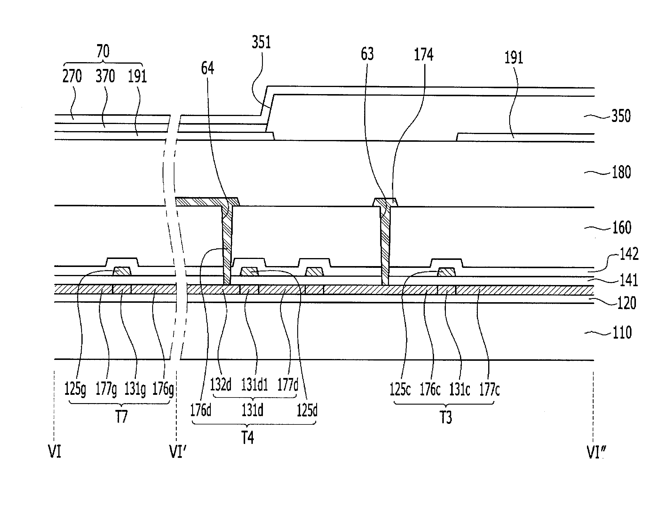
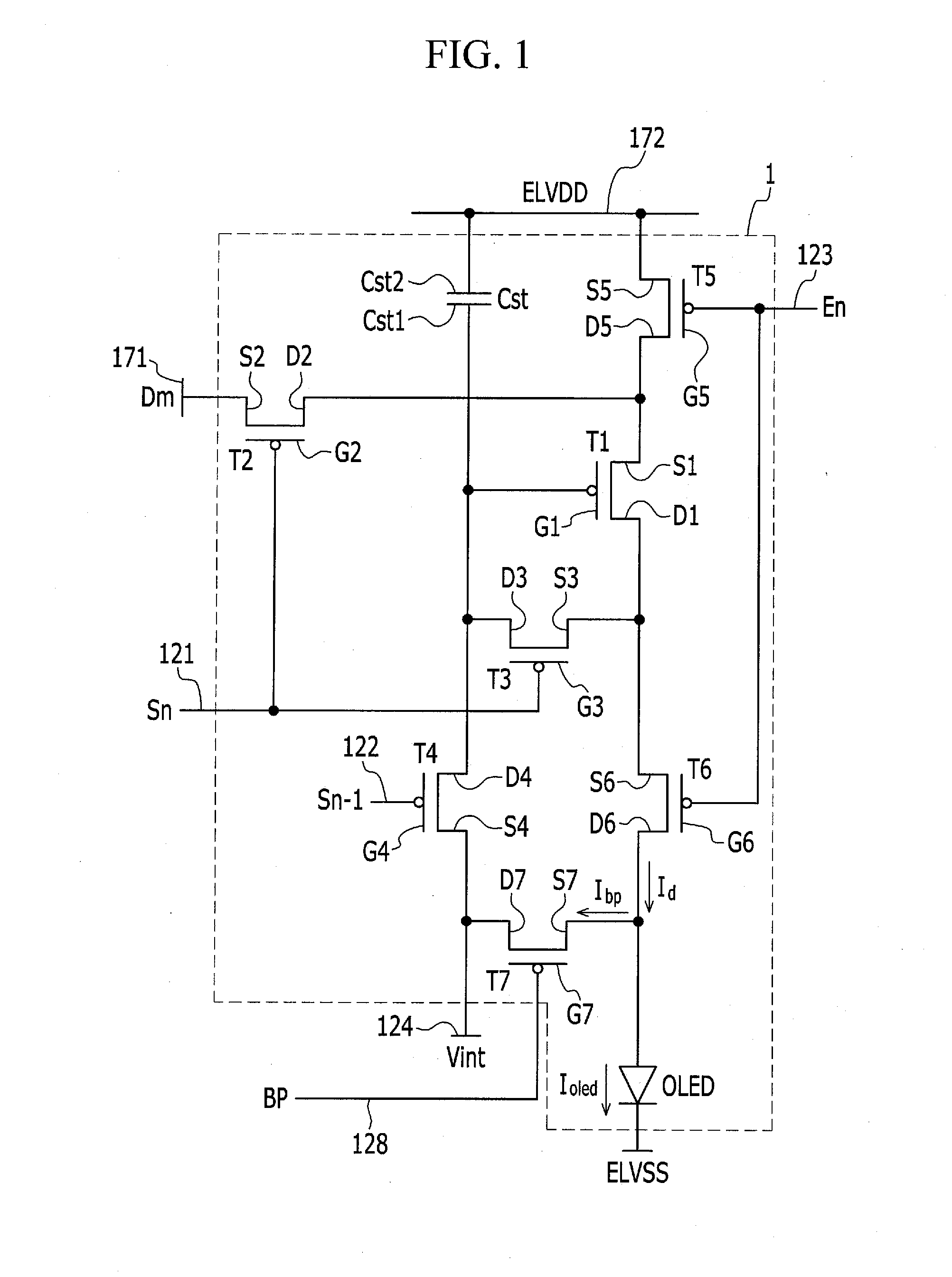
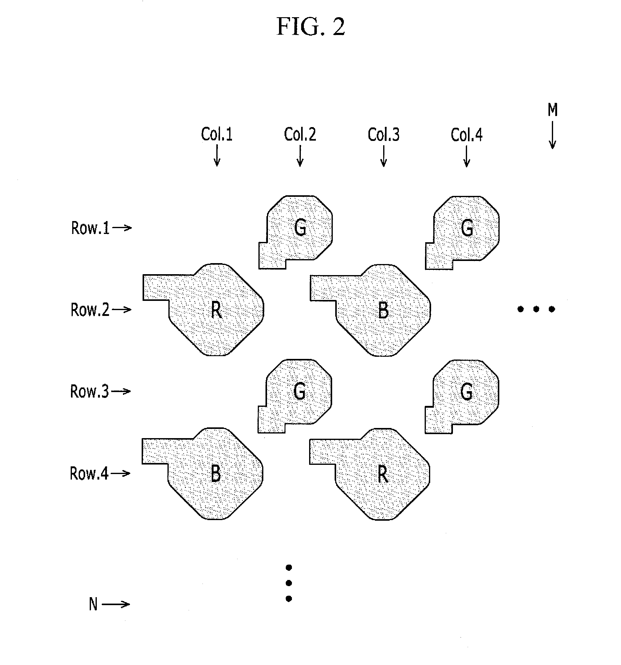
[0030]Aspects of embodiments of the present disclosure will be described hereinafter with reference to the accompanying drawings, in which example embodiments are shown. As those skilled in the art would realize, the described embodiments may be modified in various different ways, all without departing from the spirit or scope of the present disclosure.

[0031]Some of the elements and functions that are not necessary for a full understanding of the present description have been omitted to clearly describe the present disclosure, and the same elements have been designated by the same reference numerals throughout the specification.

[0032]In addition, the size and thickness of each configuration shown in the drawings are arbitrarily shown for understanding and ease of description, but the present disclosure is not limited thereto.

[0033]In the drawings, the thickness of layers, films, panels, regions, etc., are exaggerated for clarity. In the drawings, for understanding and ease of descri...


PUM


Abstract

An organic light emitting diode display includes a substrate, a scan line and a previous scan line formed on the substrate, a data line and a driving voltage line crossing the scan line and the previous scan line, a switching transistor coupled to the scan line and the data line, a driving transistor coupled to the switching transistor, a compensation transistor coupled to one end of the driving transistor and configured to compensate a threshold voltage of the driving transistor, a connecting member configured to couple a compensation semiconductor layer of the compensation transistor to a driving gate electrode of the driving transistor, a first electrode coupled to another end of the driving transistor, an organic emission layer on the first electrode, and a second electrode on the organic emission layer. The connecting member and the first electrode are spaced from each other on a planar surface of the substrate.

Description

CROSS-REFERENCE TO RELATED APPLICATION[0001]This application claims priority to and the benefit of Korean Patent Application No. 10-2013-0158198 filed in the Korean Intellectual Property Office on Dec. 18, 2013, the entire disclosure of which is incorporated herein by reference.BACKGROUND[0002]1. Field[0003]Aspects of embodiments of the present disclosure are directed to an organic light emitting diode display.[0004]2. Description of the Related Art[0005]An organic light emitting diode display includes two electrodes and an organic emission layer interposed between the two electrodes. Electrons injected from one electrode and holes injected from the other electrode are combined with each other in the organic emission layer to form excitons. Light is emitted while the excitons discharge energy.[0006]The organic light emitting diode display includes a plurality of pixels including organic light emitting diodes which are self-light emitting elements. A plurality of transistors and stor...

Claims


Application Information

Patent Timeline
IPC IPC(8): G09G3/32H01L27/32
CPCH01L27/3262H01L27/32H10K59/352H10K59/353H10K59/1213H10K59/131H01L29/786H10K59/00
Inventor BANG, HYUN-CHOL
Owner SAMSUNG DISPLAY CO LTD
Why Eureka
Try Eureka