Gate Driving Circuit And Display Panel

a driving circuit and display panel technology, applied in the field of display driving, can solve the problems of circuit failure and signal cannot be outputted, and achieve the effect of reducing the failure risk of the circuit and reducing the leakage curren

Active Publication Date: 2017-11-09
WUHAN CHINA STAR OPTOELECTRONICS TECH CO LTD
View PDF16 Cites 8 Cited by
  • Summary
  • Abstract
  • Description
  • Claims
  • Application Information

AI Technical Summary

Benefits of technology

[0014]the stabilizing circuit is connected with the pulling circuit at a second node, the input circuit responds to the scanning driving signal of the previous stage, using the first reference voltage level to set a voltage of the second node as the first voltage, and the voltage of the second node is held by the stabilizing circuit so as to reduce a leakage current between the first node and the second node; and
[0018]Wherein, the input circuit further includes a third switching tube; a control terminal of the third switching tube is connected with the first reference voltage level or the second reference voltage level, a first path terminal of the third switching tube is connected with the second path terminal of the second switching tube, a second path terminal of the third switching tube is connected with the first node, the third switching tube is turned on under an action of the first reference voltage level or the second reference voltage level in order to stabilize the voltage of the first node.
[0033]The beneficial effects of the present invention are, comparing with the conventional art, the input circuit responds to the scanning driving signal of the previous stage to set the pulling circuit as the first status, and utilizes the first reference voltage level to set the voltage of the first node at the first voltage, and held by the output circuit. The input circuit responds to the scanning driving signal of the previous stage, using the first reference voltage level to set the voltage of the second node as the first voltage, and held by the stabilizing circuit such that the output circuit output the scanning driving signal of the current stage according to the first clock signal. Through above way, the present invention set the voltage of the first node at the first voltage, and set the voltage of the second node at the same time in order to reduce the leakage current between the first node and the second node such that the voltage of the first node can be held at a magnitude within a certain time by the output circuit. When the clock signal is inputted, outputting the scanning driving signal of the current stage to reduce the failure risk of the circuit.

Problems solved by technology

If within the certain time period, the node connected with the output circuit cannot be held at the voltage magnitude because of the current leakage, the circuit will fail such that a normal gate scanning driving signal cannot be outputted.

Method used


Image

  • Gate Driving Circuit And Display Panel
  • Gate Driving Circuit And Display Panel
  • Gate Driving Circuit And Display Panel

Examples


first embodiment

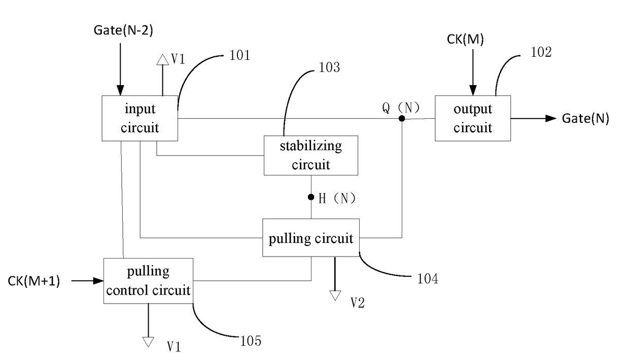
[0045]Specifically, the circuit of the present first embodiment adopts the scanning driving signal Gate(N-2) of the previous stage as a starting signal, under an action of the first clock signal CK(M), outputting the scanning driving signal Gate(N) of the current stage. Under an action of the scanning driving signal Gate(N) of the current stage, after a switch of a row of the scanning driving signal Gate(N) is written into a pixel, the scanning driving signal Gate(N) of the current stage is required to be restored in a normal status such that the switch of the row is maintained to be turned off The pulling control circuit 105 is required to be responded to the second clock signal CK(M+1) to set the pulling circuit 104 in a second status so as to use the second reference voltage level V2 to pull the voltages of the first node Q(N) and the second node H(N) and to be held at the second voltage such that the voltage of the scanning driving signal Gate(N) of the current stage is held at ...

second embodiment

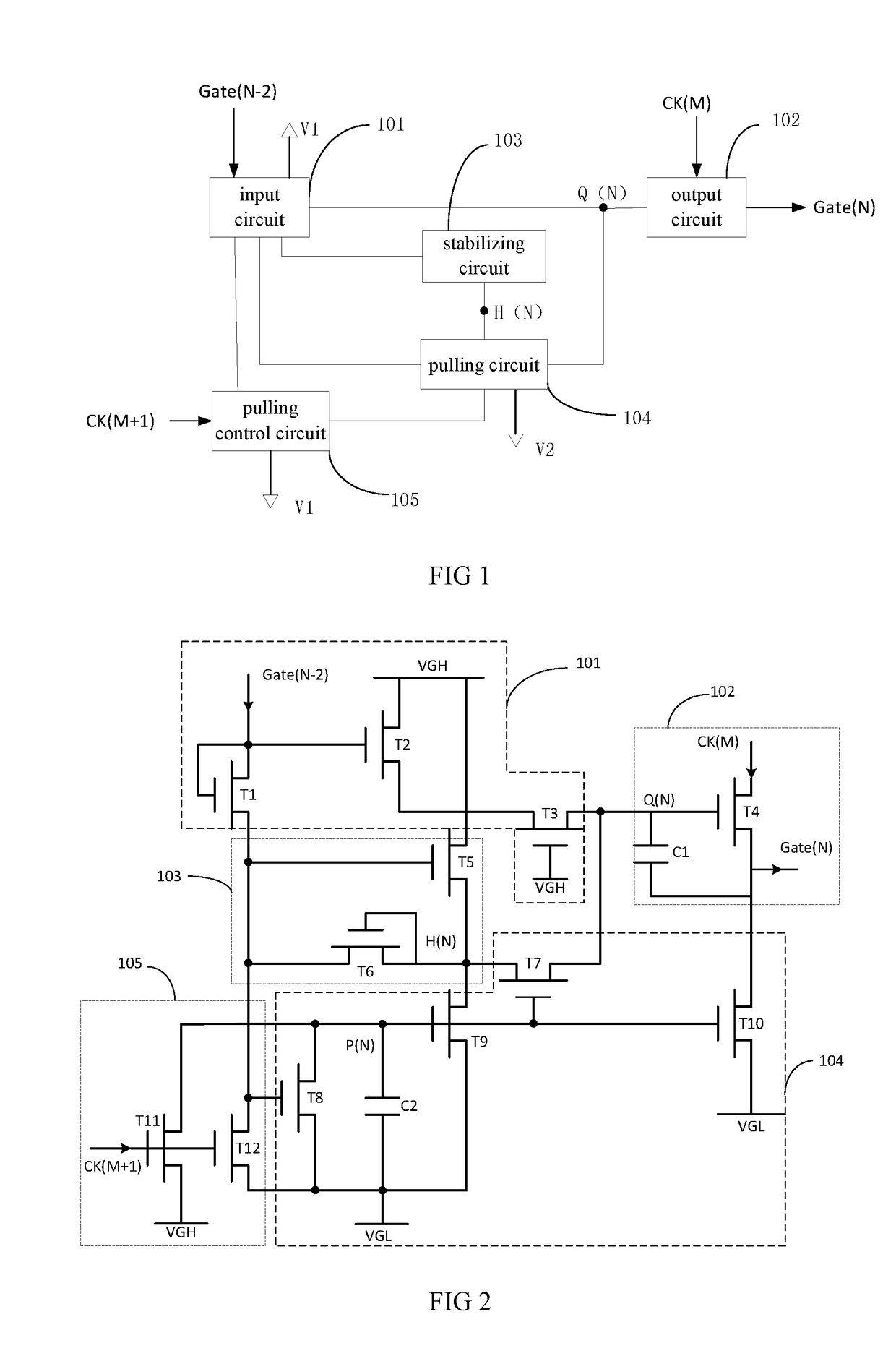
[0074]In the gate driving circuit of the present invention, using PMOS gate driving circuit designed and integrated by PMOS device to specifically describe. Wherein, a control terminal of each switching tube corresponds to a gate electrode of the PMOS transistor, a first path terminal and a second path terminal respectively correspond to a source electrode and a drain electrode of the PMOS transistor.

[0075]With reference to FIG. 5, the difference between the second embodiment and the first embodiment in FIG. 2 is, replacing all of the NMOS transistors to PMOS transistors, the first reference voltage level is the low reference voltage level VGL, the second reference voltage level is the high reference level VGH, the circuit structure is similar to the first embodiment, not repeating anymore.

[0076]FIG. 6 is a timing diagram of the gate driving circuit of the second embodiment of the present invention. Combined with FIG. 5, a specific operation process of the PMOS gate driving circuit ...

third embodiment

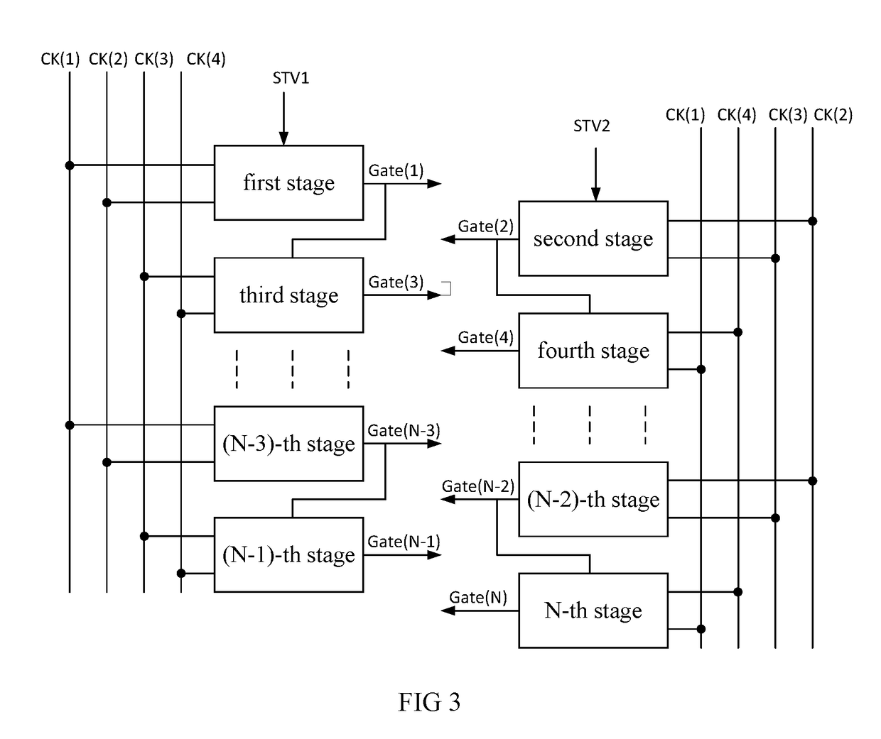
[0085]the present invention provides a display panel, including a substrate and a gate driving circuit formed on the substrate, and the gate driving circuit is the gate driving circuit provided at anyone of the above embodiments.

[0086]The first embodiment of the present invention and the second embodiment of the present invention respectively use the NMOS gate driving circuit and the PMOS gate driving circuit as examples, but not limited. In another embodiment, based on different principle for realization, the specific circuit structure of the gate driving circuit can be different, the elements in the circuit can also be different, for example, the transistor can select CMOS semiconductor device in order to meet an actual requirement.

[0087]The present invention describe a gate driving circuit and a display panel through above three embodiments, the input circuit responds to the scanning driving signal of the previous stage to set the pulling circuit as the first status, and utilizes...


PUM

PropertyMeasurementUnit
voltageaaaaaaaaaa
reference voltageaaaaaaaaaa
voltagesaaaaaaaaaa

Abstract

A gate driving circuit is disclosed. The output circuit is connected with the input circuit and the pulling circuit at a first node, responding to scanning driving signal of previous stage to set the pulling circuit in a first status, using a first reference voltage level to set the first node at a first voltage, and held. The output circuit outputs scanning driving signal of current stage according to a first clock signal. The stabilizing circuit is connected with the pulling circuit at a second node, using the first reference voltage level to set the second node at the first voltage, and held. The pulling control circuit responds to a second clock signal to set the pulling circuit in a second status, using a second reference voltage level to pull voltages of the first and second nodes and to hold the voltages. Accordingly, a current leakage can be reduced.

Description

BACKGROUND OF THE INVENTION1. Field of the Invention[0001]The present invention relates to a display driving field, and more particularly to a gate driving circuit and a display panel.2. Description of Related Art[0002]Along with the fast development of the LTPS (Low Temperature Poly-silicon) technology, integrated circuit at periphery of the panel has also become focus of people's attention. One of the very important technology is the GOA (Gate Driver On Array, array substrate row driving) technology. Using the GOA technology to integrate the gate switching circuit on the array substrate of the liquid crystal display panel in order to save a gate driving integrated circuit so as to reduce the cost from material cost and the manufacturing process.[0003]The gate switching circuit integrated on the array substrate using the GOA technology is also called as a gate driving circuit. In a traditional gate driving circuit, when controlling a gate scanning driving signal of an output circui...

Claims


Application Information

Patent Timeline
Patent Type & Authority Applications(United States)
IPC IPC(8): G09G3/36H03K17/687G02F1/1345
CPCG09G3/3677H03K17/6871G09G2320/0219G09G2300/0819G09G2300/0426G02F1/13454G09G3/3674G09G2300/0408G09G2310/0286G09G3/36
Inventor ZHAO, MANG
Owner WUHAN CHINA STAR OPTOELECTRONICS TECH CO LTD
Why Eureka
Try Eureka