
Method of manufacturing strained dislocation-free channels for CMOS
a technology of dislocation-free channels and manufacturing methods, applied in the direction of semiconductor devices, connection contact material, electrical equipment, etc., can solve the problems of higher cost, disadvantageous to the performance of pfet, and beneficial to the performance of an n
- Summary
- Abstract
- Description
- Claims
- Application Information
AI Technical Summary
Benefits of technology
Problems solved by technology
Method used
Image

Examples
Embodiment Construction
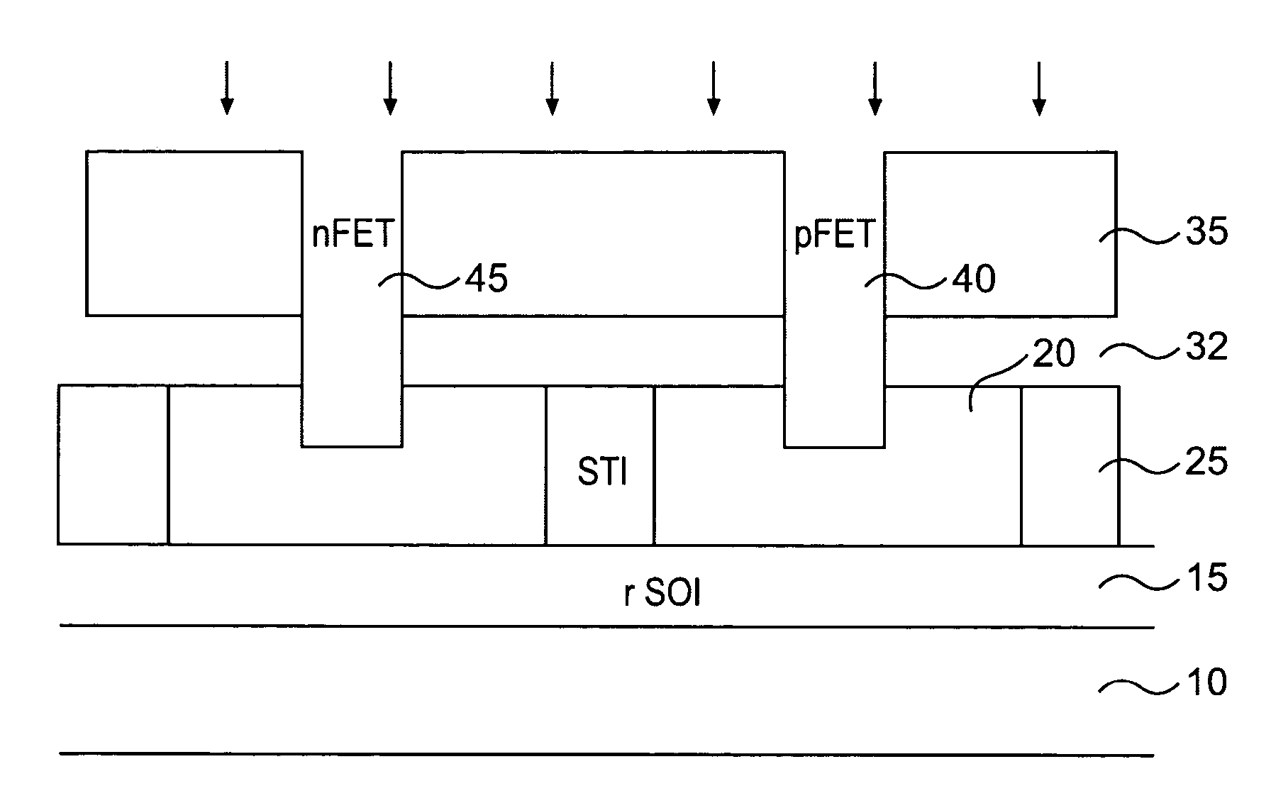
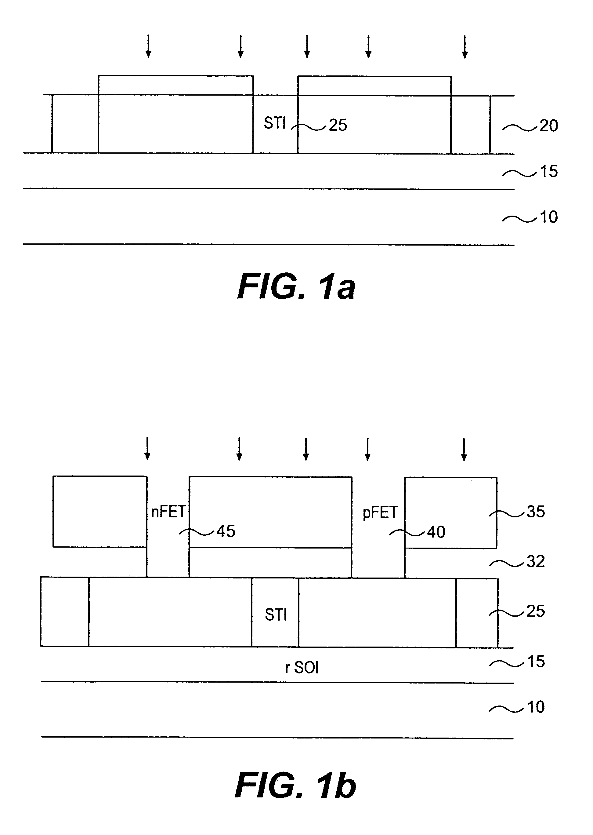
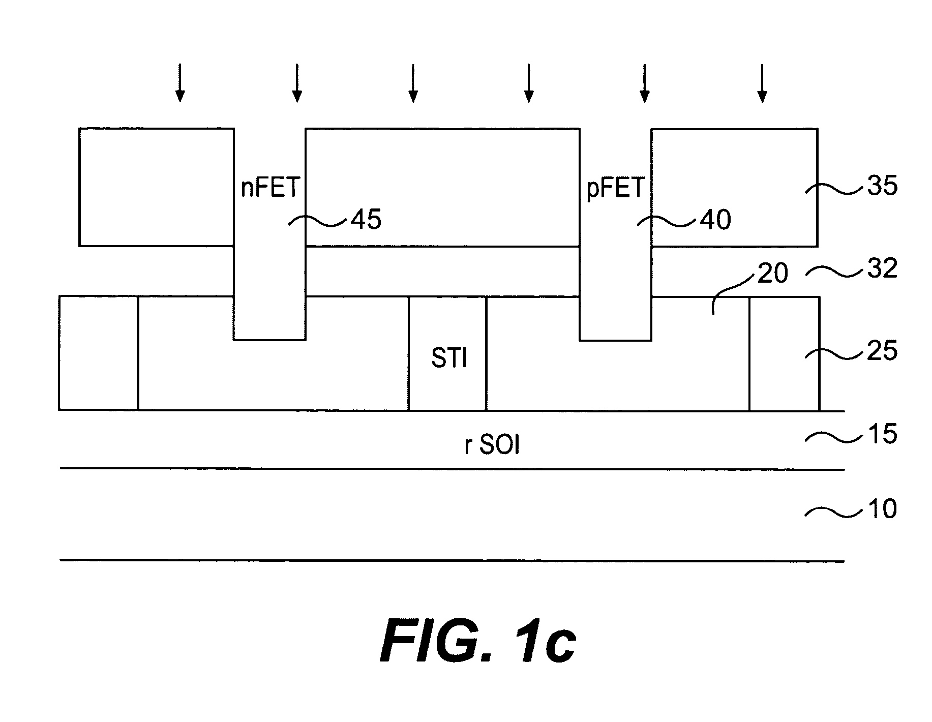
[0016]This invention is directed to a semiconductor device and method of manufacture which provides tensile stresses in the nFET channel and compressive stresses in the pFET channel of CMOS devices. In one embodiment, high tensile stresses may also be provided in the pFET channel to increase device performance. In one embodiment of the invention, channels are formed in the silicon layer in the area of the formation of the nFETs and pFETs. The channels are then filled with silicon based material having a naturally occurring lattice constant which does not match the lattice constant of the underlying silicon layer. By applying these materials, tensile and / or compressive forces result in an overlying epitaxial layer in the channels of the nFETs and pFETs, respectively. In one embodiment, the nFET and pFET channels can be formed simultaneously. By using the fabrication processes of the invention, improved device characteristics can be achieved, as well as higher yields and lower device ...
PUM
 Abstract
Description
Claims
Application Information