Imaging device

a technology of imaging device and image, which is applied in the field of imaging device, can solve the problems of image (or video) interference, picture (or video) interference, and the image device contains striped-pattern noise (beat noise), and achieve the effect of reducing the external noise and simple internal configuration

Active Publication Date: 2013-04-16
PANASONIC CORP
View PDF12 Cites 10 Cited by
  • Summary
  • Abstract
  • Description
  • Claims
  • Application Information

AI Technical Summary

Benefits of technology

[0018]As described above, according to the imaging device of the present invention, picture (or video) interference caused by external noise can be reduced without causing deterioration of the quality of a taken image even when the device is used in a strong electric field environment, and miniaturization can be achieved through having a simple internal configuration.

Problems solved by technology

When the imaging devices are used under such environments, the imaging devices may be subjected to electromagnetic wave interference.
Such an environment where the imaging devices may be subjected to electromagnetic wave interference is referred to as “a strong electric field environment.” If imaging devices such as digital still cameras and the like are used in a strong electric field environment, there are cases where picture (or video) interference occurs, such that images taken by the imaging devices contain striped-pattern noise (beat noise).
Furthermore, associated with miniaturization of the imaging devices, the amount of external strong-electric-field noise coupled to the imaging elements incorporated in the miniaturized imaging devices increases, such that the picture (or video) interference becomes more prominent.
Causes of such picture (or video) interference include penetration of external electromagnetic waves into video signal lines of the imaging elements, or fluctuation of the ground (“GND”) potential of imaging element flexible cables due to the influence of external electromagnetic waves.
However, with this measure, stress is applied on the imaging elements in the traveling direction of light, and thereby the imaging elements will tilt.
As a result, deterioration of image quality occurs in images taken by the imaging devices, and therefore it has been difficult to introduce the measure in actual products.

Method used


Image

  • Imaging device
  • Imaging device
  • Imaging device

Examples


first embodiment

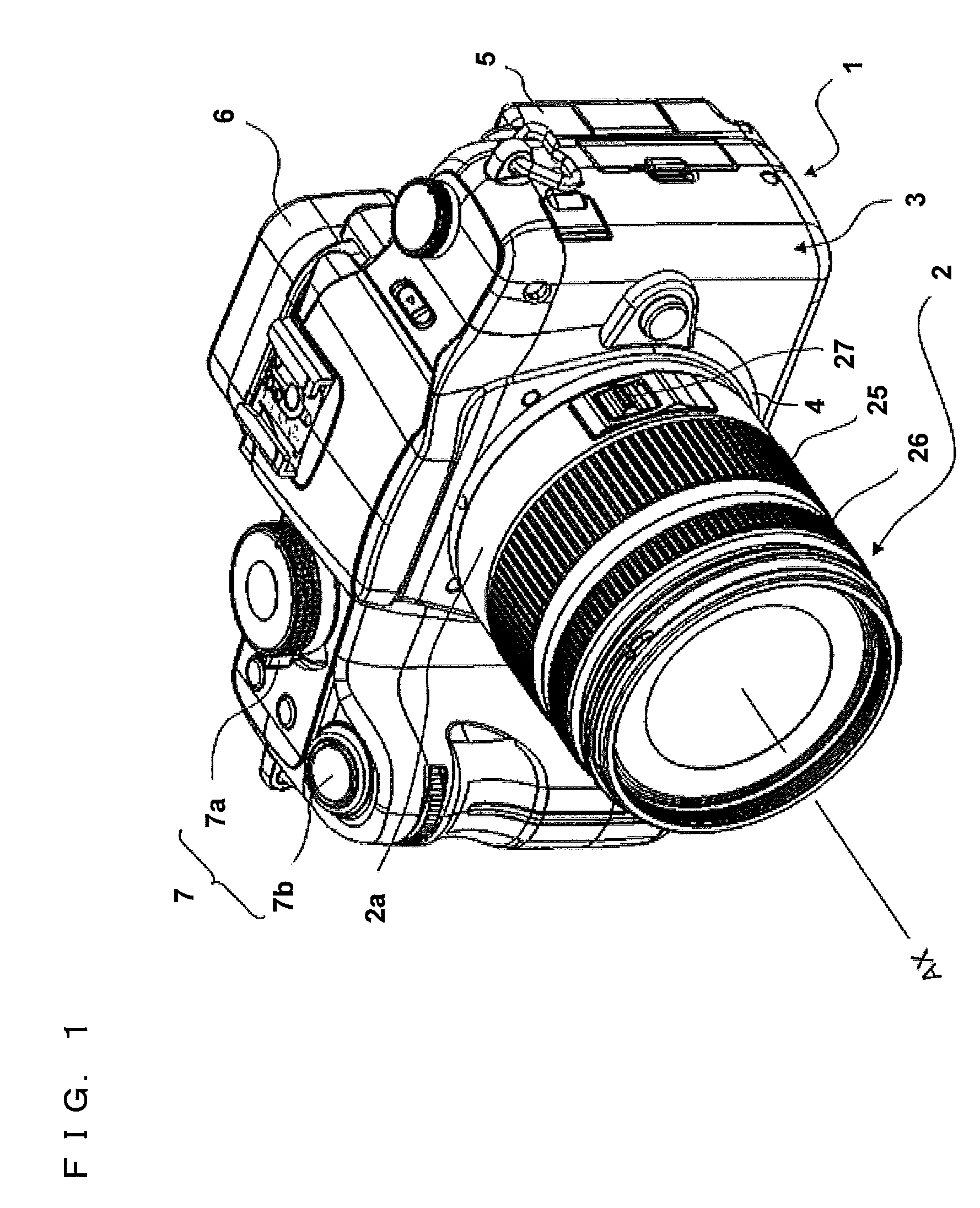
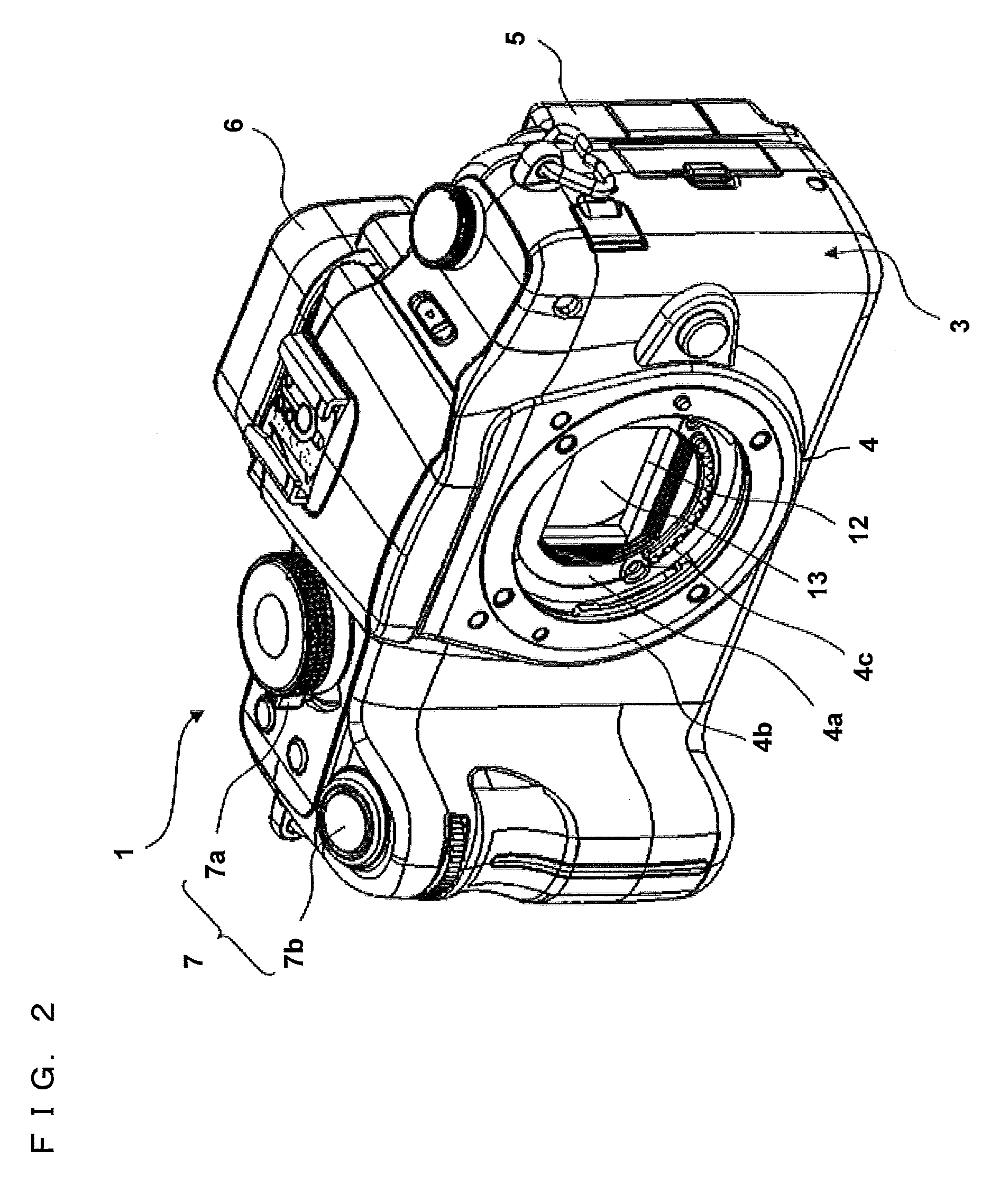
[0036]Firstly, the basic configuration of the digital camera according to the present invention will be described with reference to FIG. 1 to FIG. 4. Here, for convenience of description, the photographic-subject side of the digital camera is defined as the front, and imaging-surface side of the digital camera is defined as the back or rear.

[0037]In FIG. 1, the camera body 1 includes a main body housing 3, a body mount 4, a camera monitor 5, an electronic view finder (EVF) 6, and an operation section 7. The body mount 4 is arranged in the front surface side of the main body housing 3, and allows the interchangeable lens unit 2 to be mounted on the camera body 1. The camera monitor 5 is arranged in the back surface side of the main body housing 3, and includes a liquid crystal display, etc. The EVF 6 is arranged in the back surface side of the main body housing 3, and displays images and the like represented by display image data. The operation section 7 is arranged on an upper porti...

second embodiment

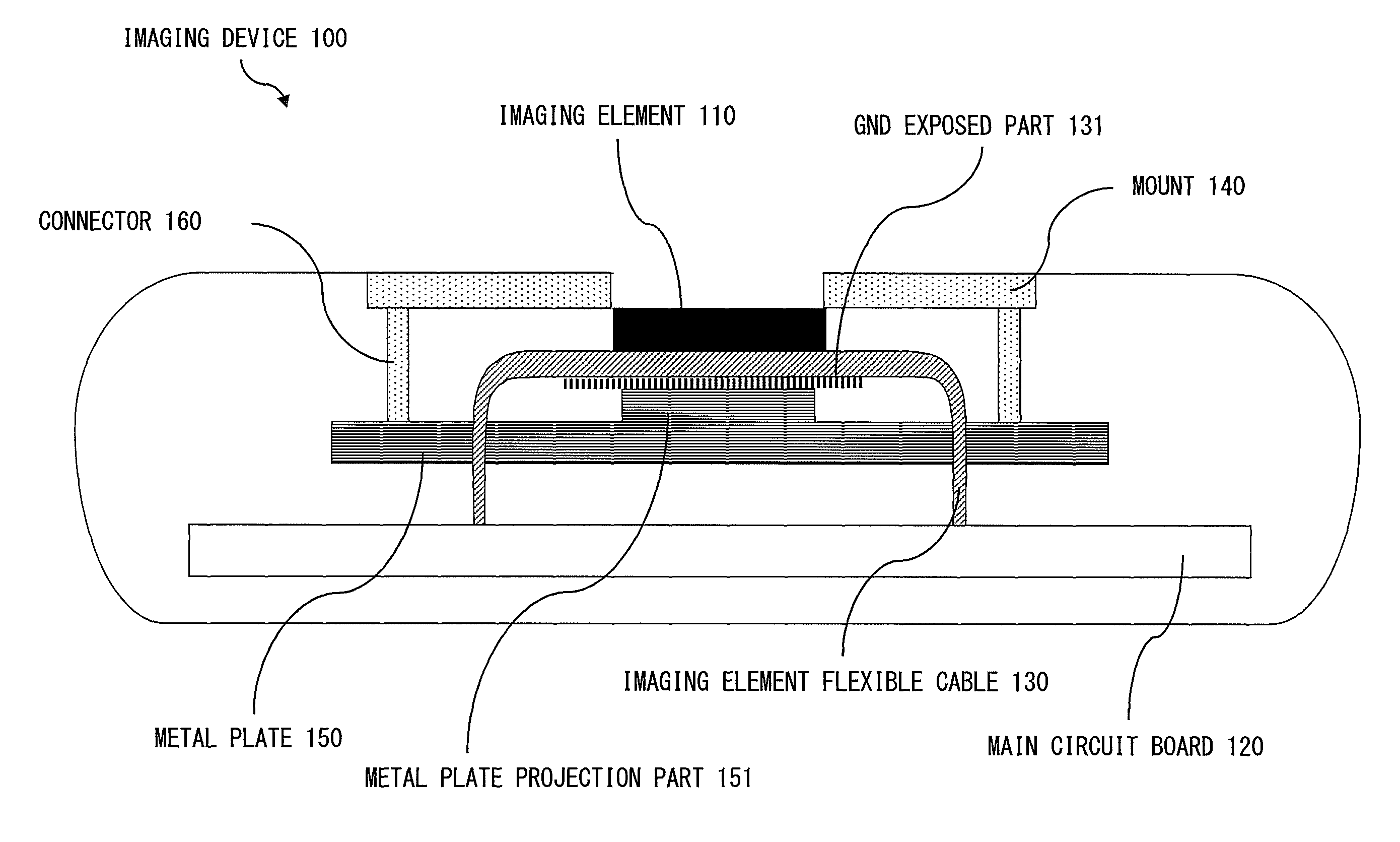
[0090]FIG. 11 is an internal structure cross sectional view of an imaging device 200 from an upper portion thereof, according to the present invention. Here, mainly, the controlling of the GND potential of the imaging element flexible cable will be described and detailed descriptions of those other than the controlling are omitted; however, the basic configuration of the imaging device 200 is similar to the configuration of the digital camera described by using FIG. 1 to FIG. 4.

[0091]In FIG. 11, the imaging device 200 includes the imaging element 110, the main circuit board 120, the imaging element flexible cable 130, the mount 140, the metal plate 150, the connector 160, and an electrically conductive elastic part 170. The imaging element flexible cable 130 includes a GND exposed part 132, and the metal plate 150 includes a metal plate concaved part 152. In FIG. 11, components identical to those of the imaging device 100 according to first embodiment of the present invention shown ...


PUM


Abstract

An imaging device of the present invention, which is an imaging device for shooting images or video of a photographic subject, includes: an imaging element for taking an optical image of the photographic subject and generating image data therefrom; a main circuit board for conducting signal processing on the image data generated by the imaging element; an imaging element flexible cable that is connected to the main circuit board and on which the imaging element is mounted; a mount for fixing the imaging element and that includes a metallic component; a metal plate disposed between the imaging element and the main circuit board. The imaging element flexible cable includes an imaging element flexible cable GND which has a ground potential, and the imaging element flexible cable GND is connected to the metal plate.

Description

TECHNICAL FIELD[0001]The present invention relates to imaging devices such as digital still cameras and the like, and more specifically, relates to imaging devices for reducing picture (or video) interference caused by external noise.BACKGROUND ART[0002]In recent years, occasions in which imaging devices such as digital still cameras and the like are employed in environments where electromagnetic wave-radiating handheld information terminals such as mobile phones and PHS's (Personal Handyphone Systems) are used are increasing. In addition, occasions in which imaging devices such as digital still cameras and the like are employed in environments, including the vicinity of radio broadcasting stations and television broadcasting stations, for example, where strong electromagnetic waves are radiated are also increasing.[0003]When the imaging devices are used under such environments, the imaging devices may be subjected to electromagnetic wave interference. Such an environment where the ...

Claims


Application Information

Patent Timeline
Patent Type & Authority Patents(United States)
IPC IPC(8): H04N5/225
CPCH04N5/2253H04N23/54
Inventor TOBINAGA, MASATOFUSAYASU, HIROTSUGUKUMOI, MASAFUMI
Owner PANASONIC CORP
Why Eureka
Try Eureka