
Charge pump circuit and integrated circuit
A charge pump and circuit technology, applied in electrical components, conversion equipment without intermediate conversion to AC, and output power conversion devices, etc., can solve problems such as non-resistance of electrostatic discharge, reduce leakage current, reduce on-chip area, The effect of improving performance
Patent Information
- Authority / Receiving Office
- CN · China
- Patent Type
- Applications(China)
- Current Assignee / Owner
- Publication Date
- 2008-12-03
- Estimated Expiration
- Not applicable · inactive patent
Smart Images
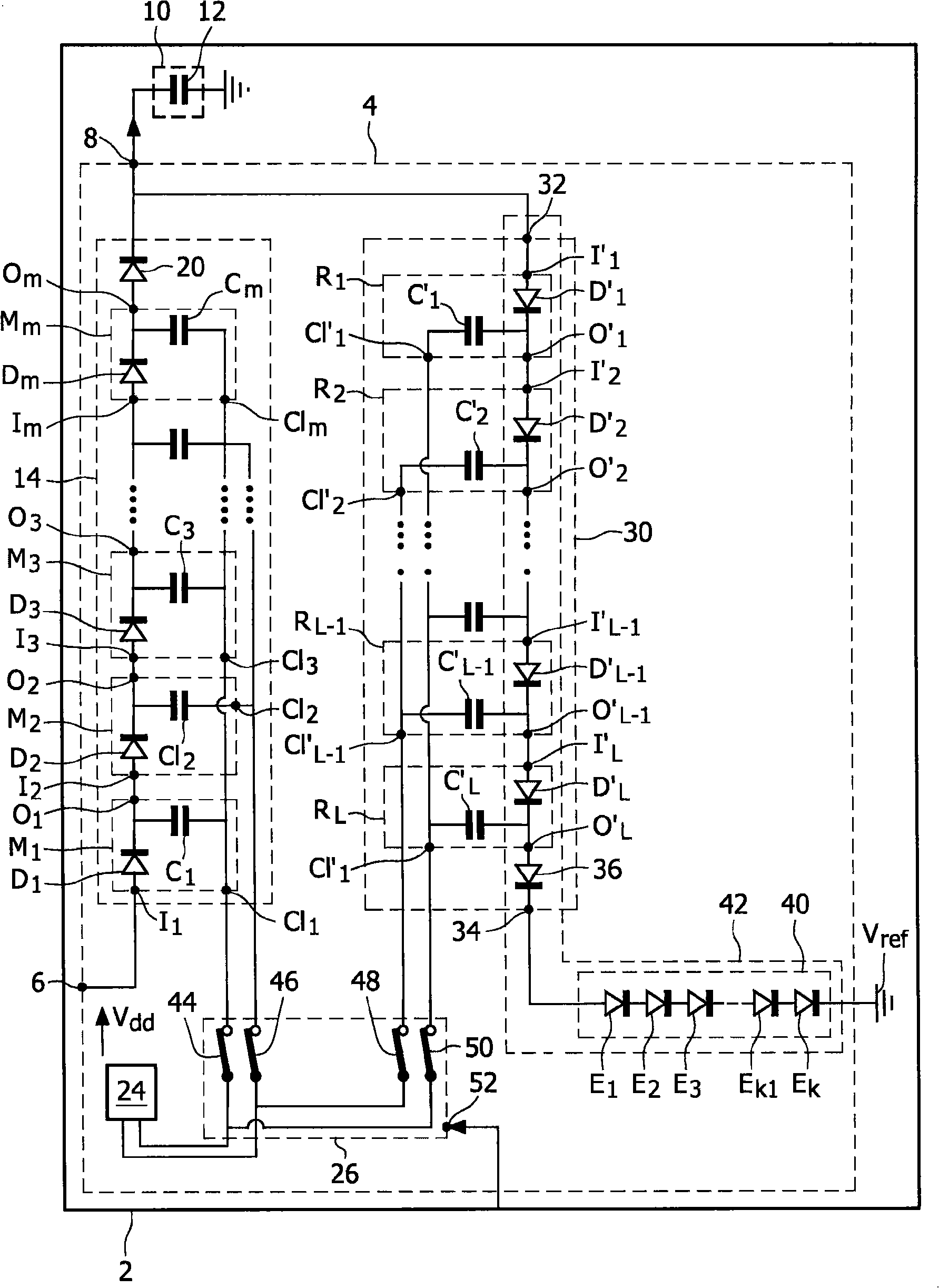
Figure 1 
Figure 2 
Figure 3
Abstract
Description
technical field
[0001] The invention relates to a charge pump circuit and an integrated circuit. Background technique
[0002] Typically, a charge pump circuit for boosting a DC voltage circuit can include:
[0003] - a DC-DC boost converter having an array of capacitors for boosting the circuit voltage to a higher voltage, a DC-DC boost converter having an output lead for outputting the higher voltage, and
[0004] - A DC-DC buck converter connected to the output lead, the DC-DC buck converter having an array of capacitors and diodes for stepping down the higher voltage.
[0005] The DC-DC boost converter also has a diode that prevents current from being drawn from the output lead through the DC-DC boost converter.
[0006] Current sinking through the DC-DC buck converter is only possible when the DC-DC buck converter is activated. The DC-DC buck converter may only be activated when the DC-DC boost converter is disabled.
[0007] Therefore, the circuit described above d...
Examples
Embodiment Construction
[0032] figure 1 An integrated circuit 2 is shown. Hereinafter, no detailed description will be given for functions or structures that are well known to those skilled in the art.
[0033] More precisely, figure 1 A portion of the on-chip area of an integrated circuit is shown, where a charge pump circuit 4 is implemented to boost the DC circuit voltage V dd .
[0034] Circuit 4 has a function for receiving the voltage V dd The input leads 6 and for the output higher DC voltage V OUT output leads 8.
[0035] The leads 8 are connected to an on-chip load 10 . For example, load 10 is a capacitive load with capacitor 12 .
[0036] A DC-DC boost converter 14 is connected directly between leads 6 and 8 to boost lead 8 to a higher voltage V OUT .
[0037] Converter 14 is, for example, a Dickson charge pump converter. Such converters are described, for example, in the following references:
[0038] "On-chip high-voltage generation in MNOS integrated circuits using an improv...