
A kind of field effect organic solar cell and preparation method thereof
A solar cell and field effect technology, applied in circuits, photovoltaic power generation, electrical components, etc., can solve the problems of low open circuit voltage, low light energy, and no practical value of devices
Patent Information
- Authority / Receiving Office
- CN · China
- Patent Type
- Patents(China)
- Current Assignee / Owner
- Publication Date
- 2018-01-19
Smart Images
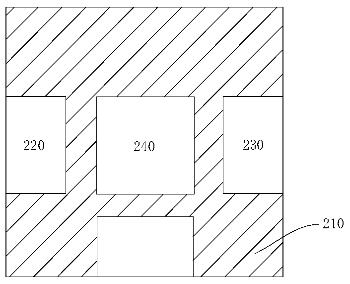
Figure 1 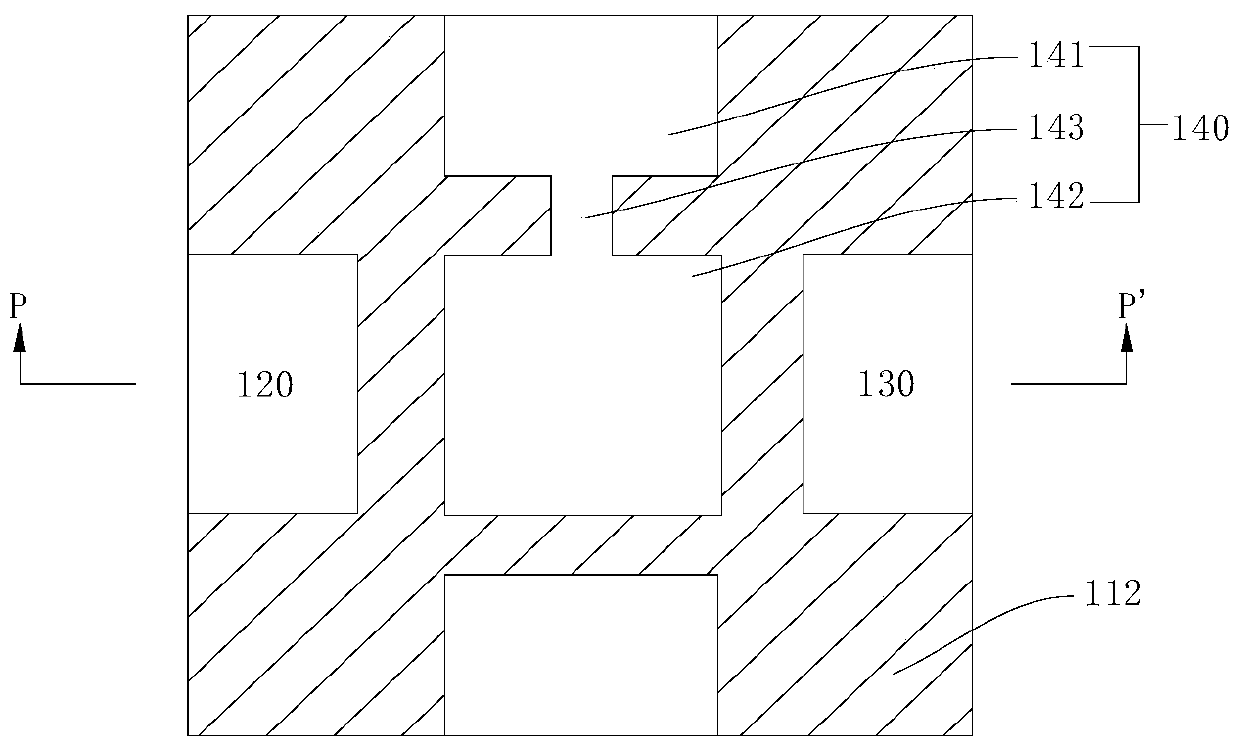
Figure 2 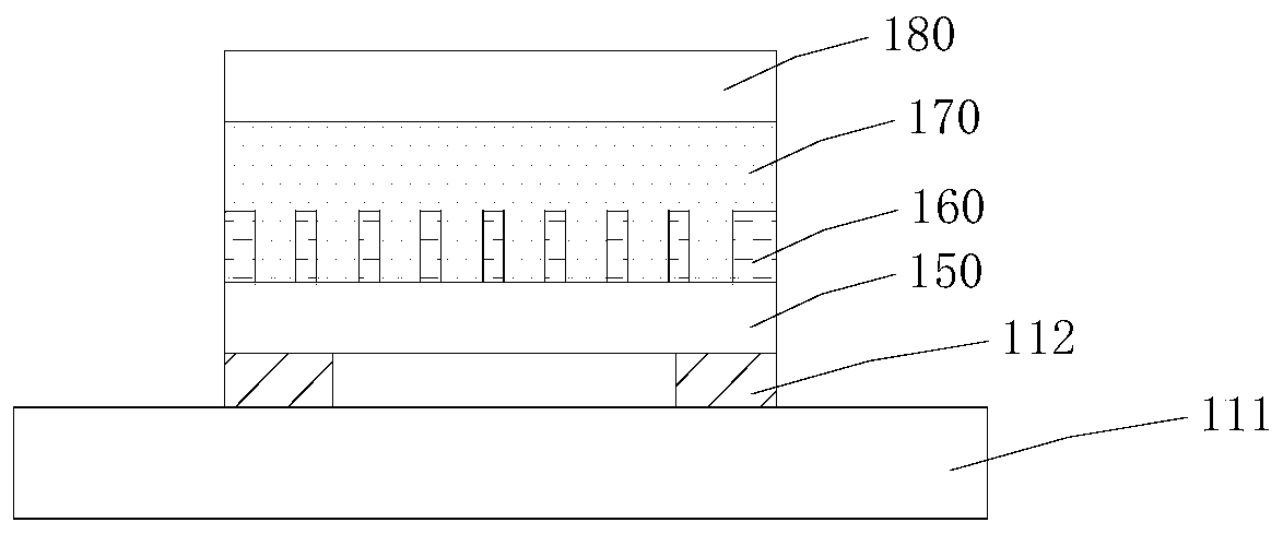
Figure 3
Abstract
Description
technical field
[0001] The invention relates to the technical field of photovoltaic devices such as solar cells, in particular to a field-effect solar electrode and a preparation method thereof. Background technique
[0002] Organic solar cells have the advantages of flexibility, low cost, and large-area preparation. They have huge market prospects and have become a hot spot for academic research and industrial development. From the perspective of practical application, the photoelectric conversion efficiency of laboratory organic solar cells needs to reach at least 10%, and the life span of more than 7 years is possible to try mass production and commercial application. In recent years, the improvement of the efficiency of organic solar cells has achieved very encouraging results. Several research groups have reported >8% efficiency. In 2012, some groups have reached the device efficiency threshold of 10%. From a research point of view, thermodynamic theory analysis bel...
Examples
Embodiment 1
[0031] Existing field-effect organic solar cells, such as figure 1 As shown, the anode electrode 220 , cathode electrode 230 and gate electrode 240 etched on the substrate 210 are included. The gate electrode 240 is generally located at the center of the substrate 210 . This structure is not conducive to the open circuit voltage V oc , short-circuit current J sc and an increase in fill factor FF.
[0032] This embodiment provides a field effect organic solar cell, such as figure 2 As shown, it includes an anode electrode 120 etched on the substrate, a cathode electrode 130 and a gate electrode 140, wherein the gate electrode 140 is an improvement on the gate electrode 240 of the prior art, in order to distinguish it from the existing gate electrode 240, The present invention is named "gate electrode". Thus, the solar cell of the present invention comprises from bottom to top: substrate 110 etched with anode electrode 120 and cathode electrode 130 , dielectric layer 150 ,...
Embodiment 2
[0048] The difference between this embodiment and Embodiment 1 is that each electrode pattern is prepared on the substrate by photolithography. Then use HCl and Zn powder to perform wet etching on the place not protected by photoresist. Alternatively, argon ion beam etching (IBE) is used to perform dry etching on the substrate without photoresist protection. An 80nm-thick Al2O3 is grown on the pair of gate electrodes by atomic deposition as the dielectric layer of the device. The PEDOT films grown on other substrates were peeled off and transferred onto the dielectric layer in ethanol.
[0049] Other procedures are identical with embodiment 1.
Embodiment 3
[0051] The difference between this embodiment and Embodiment 1 is that each electrode pattern is etched out with the aid of a mask plate by argon ion beam etching (IBE). Spin-coat 800 nm thick polyimide (PI) on the gate electrode pair as the dielectric layer of the device. A grid pattern is etched on the dielectric layer by photolithography, and then a layer of ITO electrode material with a thickness of 200 nanometers is sputtered to prepare a grid anode layer.
[0052] Other procedures are identical with embodiment 1.