
Compound type multilayer film structure silver nanowire and preparation method thereof
A technology of silver nanowires and multi-layer films, applied in nanotechnology, nanotechnology, nanotechnology for materials and surface science, etc., can solve the problems of high requirements for reaction equipment, large energy consumption, complex process, etc., and achieve cost Low cost, less time-consuming, high-purity results
Patent Information
- Authority / Receiving Office
- CN · China
- Patent Type
- Applications(China)
- Current Assignee / Owner
- Publication Date
- 2016-08-10
- Estimated Expiration
- Not applicable · inactive patent
Smart Images
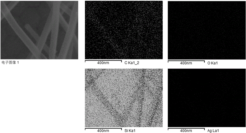
Figure 1 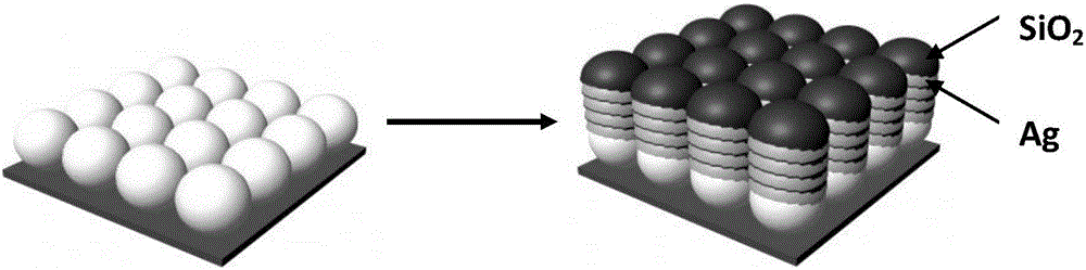
Figure 2 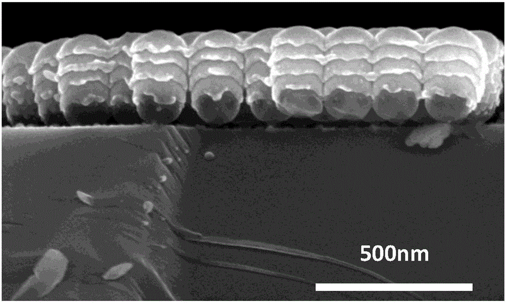
Figure 3
Abstract
Description
technical field
[0001] The invention belongs to the technical field of nano functional materials. Background technique
[0002] Nanomaterials have many unique properties and special applications. The particularity of their structure leads to macroscopic physical effects of sound, light, electricity, magnetism, heat, mechanics, etc. that are different from conventional materials, which are reflected in quantum size effects, Small size effect, surface effect and macroscopic tunnel effect have become the hotspots of current research. Nanomaterials have a low light reflection coefficient, can efficiently convert solar energy into electrical energy and heat energy, and as additives can also enhance toughness and strength, and have huge development space in the fields of electronics, magnetism, acoustics, optics, etc. and potential value. As a one-dimensional inorganic nanomaterial, silver nanowires have been widely used in the fields of polarizing devices, photonic crystals, ca...
Examples
Embodiment 1
[0020] First, a single-layer two-dimensional ordered colloidal ball template was prepared by self-assembly technology. figure 1 Middle a is the schematic diagram of colloidal ball template. The specific steps are: put the silicon wafer substrate into a mixed solution containing ammonia, hydrogen peroxide and water (volume ratio 1:2:6) and boil for five minutes, then ultrasonically clean it three times with deionized water and ethanol solution successively. One of the silicon wafers was soaked in 10% sodium lauryl sulfate solution for 24 hours to obtain a hydrophilic substrate surface, and the rest were stored in deionized water to be used as colloidal ball template substrates. Take a polystyrene solution with a volume ratio of 1:1 and mix it with deionized water, and then take a drop of the mixed solution and drop it on the silicon wafer substrate soaked in the sodium lauryl sulfate solution. After the solution is evenly diffused, slowly Immerse it in a container filled with ...
Embodiment 2
[0025] The difference between this embodiment and embodiment 1 is that the magnetron sputtering technology is used to sequentially deposit 20-30nm silver and 3-5nm silicon dioxide on the two-dimensional ordered colloidal sphere template, and the cyclic deposition period can be 1~ 5 cycles. The technical effect achieved is the same as that of Embodiment 1.
Embodiment 3
[0027] The difference between this embodiment and embodiment 1 is that [Ag 30nm / SiO 2 5nm] n The nano-multilayer film array is immersed in tetrahydrofuran, chloroform, toluene and other organic solvents to remove the polystyrene two-dimensional ordered colloidal ball sequence template. The technical effect achieved is the same as that of Embodiment 1.