
Bulk doped diamond-base normally-off field effect transistor and preparation method thereof
A technology of field effect transistors and diamonds, applied in the direction of transistors, semiconductor/solid-state device manufacturing, semiconductor devices, etc., can solve the problems of channel electrical performance degradation and disappearance, and achieve non-degradation of working characteristics and strong carrier depletion ability Effect
Patent Information
- Authority / Receiving Office
- CN · China
- Patent Type
- Applications(China)
- Current Assignee / Owner
- Publication Date
- 2019-02-22
Smart Images
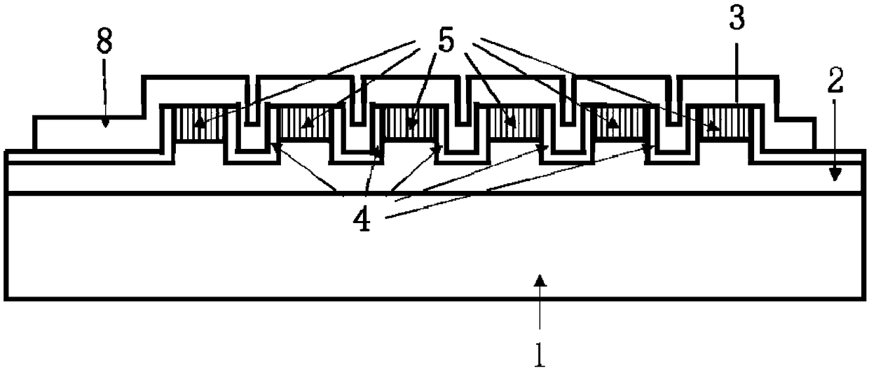
Figure 1 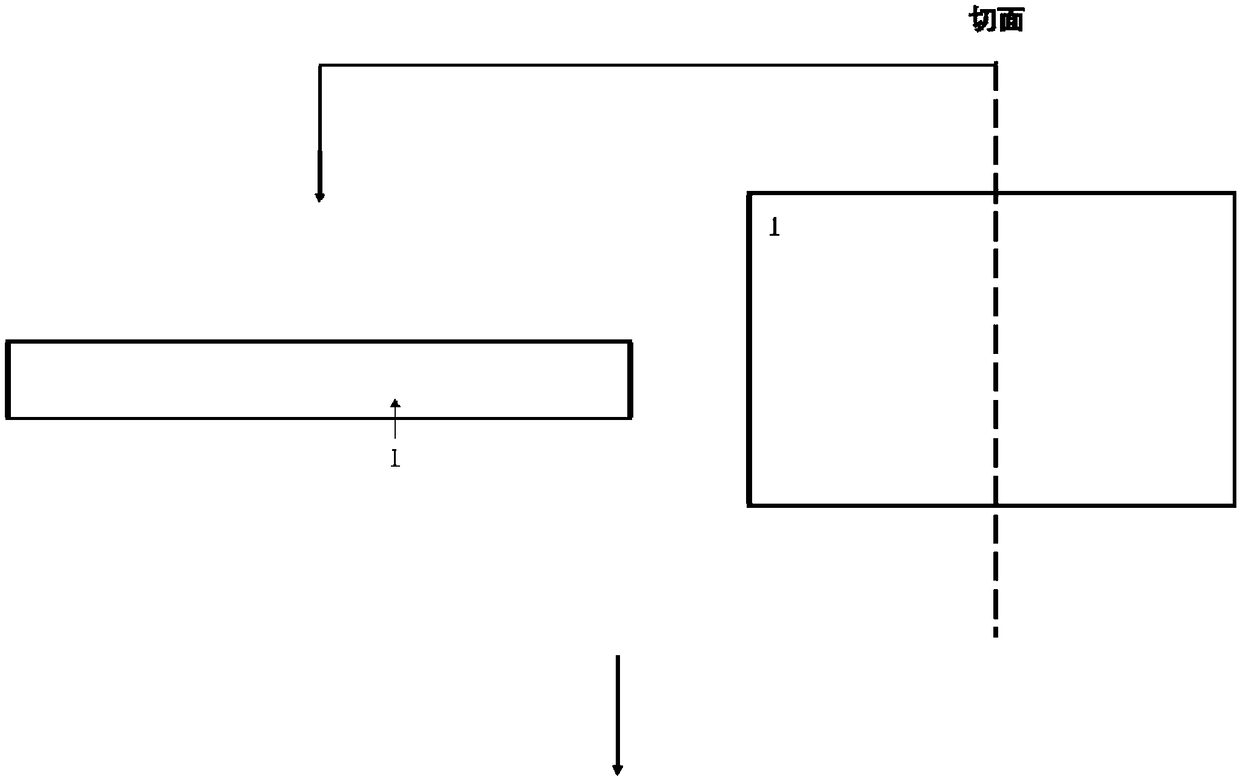
Figure 2 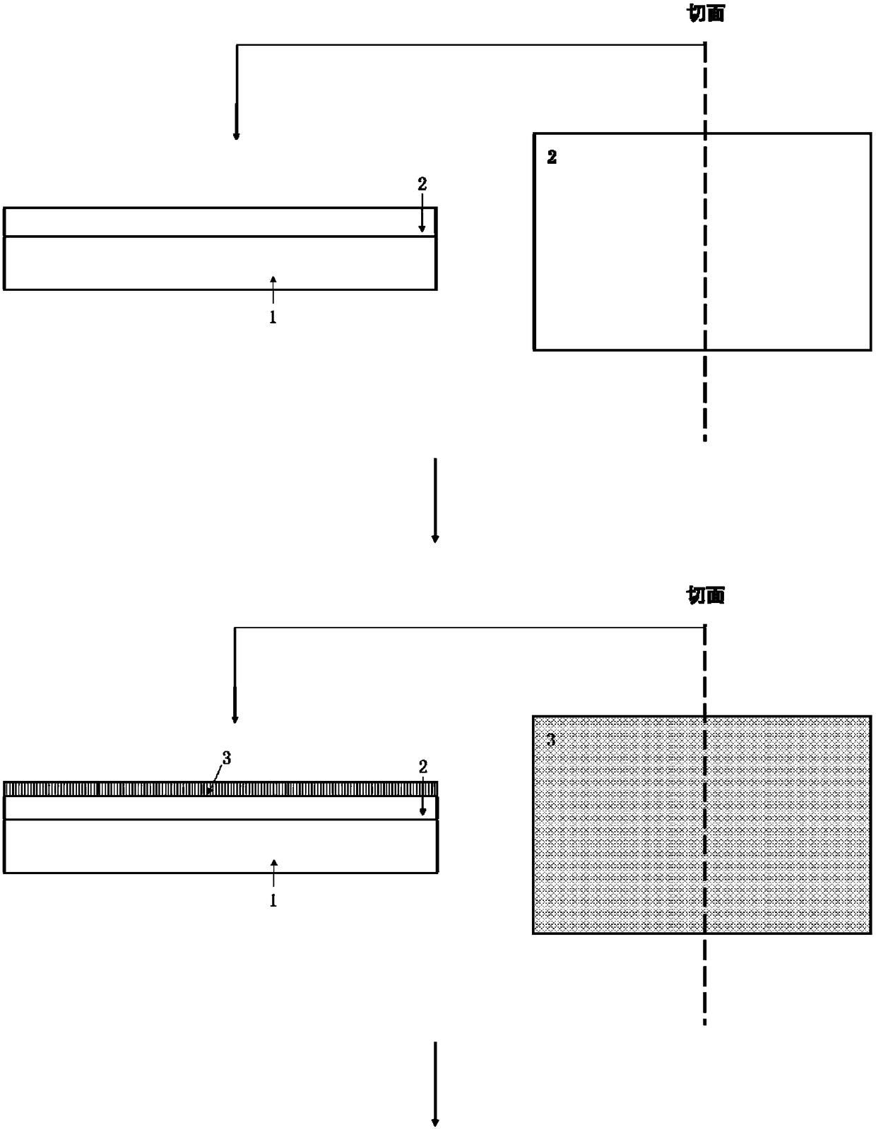
Figure 3
Abstract
Description
Technical field
[0001] The invention belongs to the technical field of semiconductor devices, and particularly relates to a normally-off diamond-based field effect transistor and a preparation method thereof. Specifically, it relates to a body-doped diamond-based normally-off field-effect transistor and a preparation method thereof. Background technique
[0002] Semiconductor single crystal materials have gone through four generations of development. The first generation of Si and Ge semiconductors brought mankind into the information age, and also promoted the intelligence and informatization of electronic systems. The second generation of semiconductors (GaAs, InP, MCT, etc.) has brought us optoelectronic devices, power electronic devices, radio frequency electronic devices and space anti-radiation devices, etc., triggering revolutions in the information fields such as wireless communications and optical communications. The third generation of wide bandgap semiconductors ...
Examples
Embodiment 1
[0051] A method for preparing a bulk-doped diamond-based normally-off field-effect transistor, comprising the following steps:
[0052] 1) The diamond substrate 1 grown by high temperature and high pressure (HPHT) technology is cleaned successively by using the standard cleaning process for diamond substrates, followed by inorganic and organic cleaning, and blown dry with nitrogen gas for later use.
[0053] 2) Deposit a single crystal diamond film 2 on the cleaned diamond substrate using microwave plasma vapor chemical deposition (MPCVD), the plasma power is 1kW, the chamber pressure is 100Torr, and the total gas flow is 500sccm, and the obtained single crystal diamond The thickness of the film is 1μm, the resistivity is greater than 100MΩ·cm, the root mean square surface roughness is less than 0.5nm, and the half-peak width of the Raman curve is less than 2cm -1 , XRD rocking curve half width less than 30arcsec.
[0054] 3) The diamond sample remains in the MPCVD chamber, t...
Embodiment 2
[0059] A method for preparing a bulk-doped diamond-based normally-off field-effect transistor, comprising the following steps:
[0060] 1) The diamond substrate 1 grown by high temperature and high pressure (HPHT) technology is cleaned successively by using the standard cleaning process for diamond substrates, followed by inorganic and organic cleaning, and blown dry with nitrogen gas for later use.
[0061] 2) Deposit a single crystal diamond film 2 on the cleaned diamond substrate using microwave plasma vapor chemical deposition (MPCVD), the plasma power is 1kW, the chamber pressure is 100Torr, and the total gas flow is 500sccm, and the obtained single crystal diamond The thickness of the film is 1μm, the resistivity is greater than 100MΩ·cm, the root mean square surface roughness is less than 0.5nm, and the half-peak width of the Raman curve is less than 2cm -1 , XRD rocking curve half width less than 30arcsec.
[0062] 3) The diamond sample is taken out and placed in a DC...
Embodiment 3
[0067] A method for preparing a bulk-doped diamond-based normally-off field-effect transistor, comprising the following steps:
[0068] 1) The diamond substrate 1 grown by high temperature and high pressure (HPHT) technology is cleaned successively by using the standard cleaning process for diamond substrates, followed by inorganic and organic cleaning, and blown dry with nitrogen gas for later use.
[0069] 2) Deposit a single crystal diamond film 2 on the cleaned diamond substrate using microwave plasma vapor chemical deposition (MPCVD), the plasma power is 1kW, the chamber pressure is 100Torr, and the total gas flow is 500sccm, and the obtained single crystal diamond The thickness of the film is 1μm, the resistivity is greater than 100MΩ·cm, the root mean square surface roughness is less than 0.5nm, and the half-peak width of the Raman curve is less than 2cm -1 , XRD rocking curve half width less than 30arcsec.
[0070] 3) The diamond sample is taken out and placed in the ...