
TVS device based on SOI substrate and manufacturing method thereof
A substrate and device technology, which is applied in TVS devices based on SOI substrates and its manufacturing field, can solve the problems of unbalanced TVS, easy loss of high-frequency signals, large leakage current and large capacitance, etc. Low leakage current, low clamping voltage, effect of low clamping voltage
Patent Information
- Authority / Receiving Office
- CN · China
- Current Assignee / Owner
- Publication Date
- 2020-02-11
Smart Images
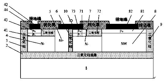
Figure 1 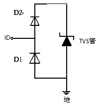
Figure 2 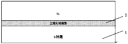
Figure 3
Abstract
Description
technical field
[0001] The invention relates to the technical field of semiconductor device manufacturing, in particular to a TVS device based on an SOI substrate and a manufacturing method thereof. Background technique
[0002] TVS (Transient Voltage Suppressor) device is a clamp overvoltage protection device, which can fix the surge voltage at a relatively low voltage level in a short period of time, so that the back-end integrated circuits are protected from over-surge Voltage shock to avoid damage to it. TVS devices are mainly used in various interface circuits, such as mobile phones, tablets, TV sets, and computer hosts, which have a large number of TVS protection devices. At present, with the continuous development of integrated circuits IC in the direction of miniaturization, low voltage, and low power consumption, corresponding performance requirements are also put forward for the corresponding TVS protection devices, that is, the clamping voltage of TVS is required...
Examples
Embodiment Construction
[0051] A TVS device based on SOI substrate, such as figure 1 As shown, an SOI substrate 1 is adopted, and its basic unit is composed of a silicon dioxide buried layer 2 and a deep groove of silicon dioxide to form an isolation layer. The surface of the silicon dioxide buried layer has a first silicon dioxide deep groove 3, The first N-region 4, the N+ region 5, the second silicon dioxide deep groove 6, the second N-region 7, the NW region 8 and the third silicon dioxide deep groove 9, wherein,
[0052] The thickness of the silicon dioxide buried layer is not less than 6000Å;
[0053] On the surface of the first N-region 4, there are doped first P-region 41, first silicon dioxide shallow groove 42 in sequence, and on the surface of the second N-region 7, there are doped second P-region 71, the first Silicon dioxide shallow groove 72, and doped on the first and second P-regions 41 and 71 surfaces to form first and second P+ regions 43 and 73 respectively, forming two P+ / P- / N- r...