
Method for manufacturing a floating gate of a dual gate of semiconductor device
Patent Information
- Authority / Receiving Office
- US · United States
- Current Assignee / Owner
- Publication Date
- 2004-11-11
- Estimated Expiration
- Not applicable · inactive patent
Smart Images
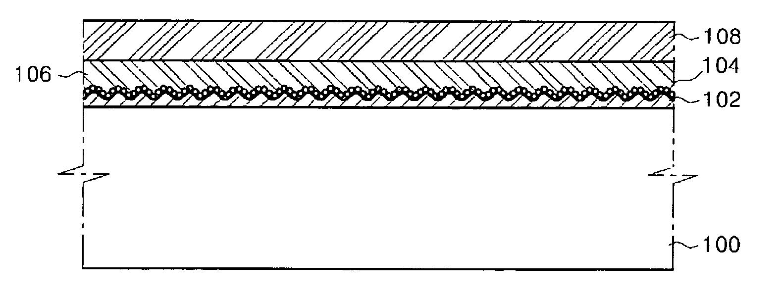
Figure 1 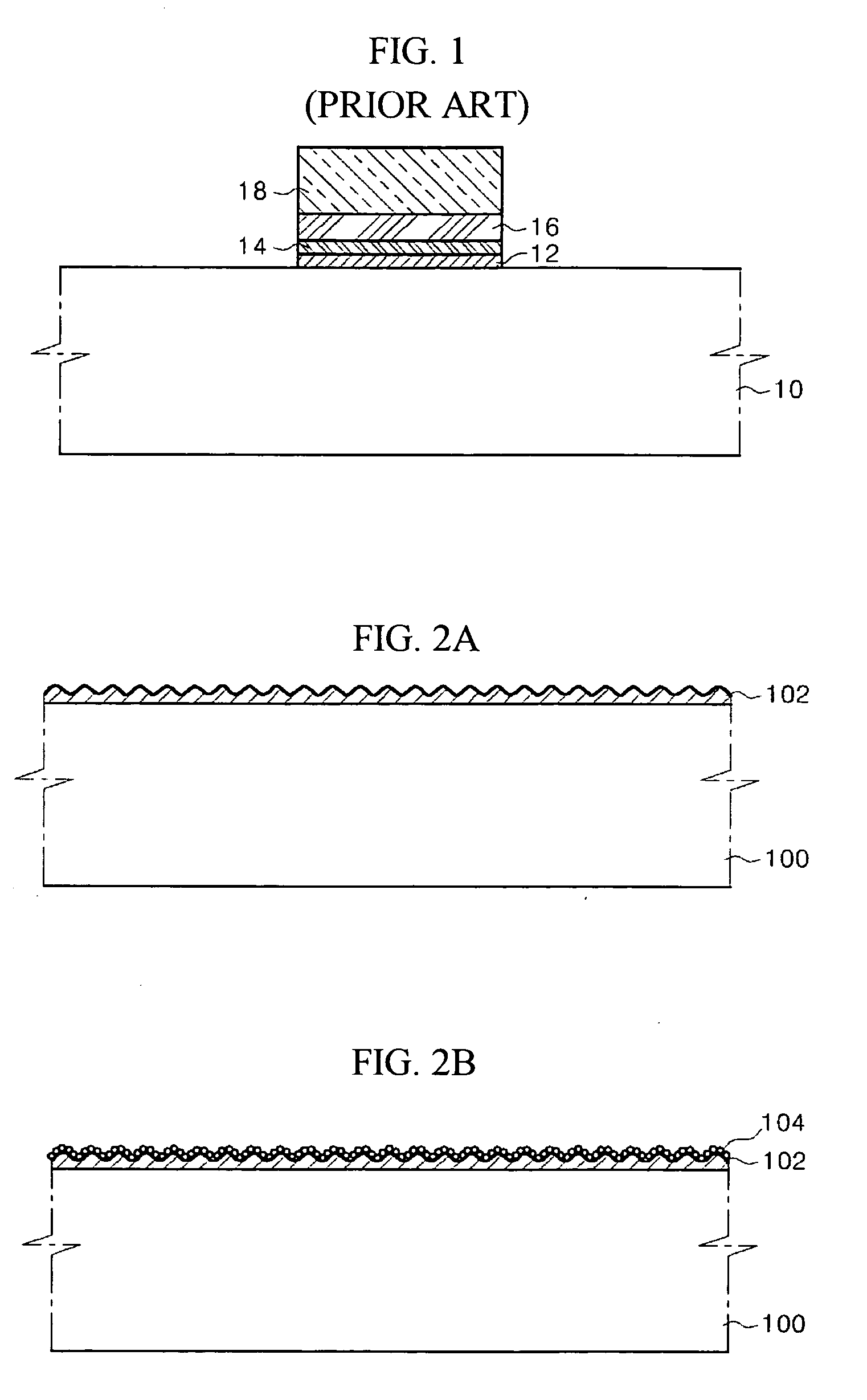
Figure 2 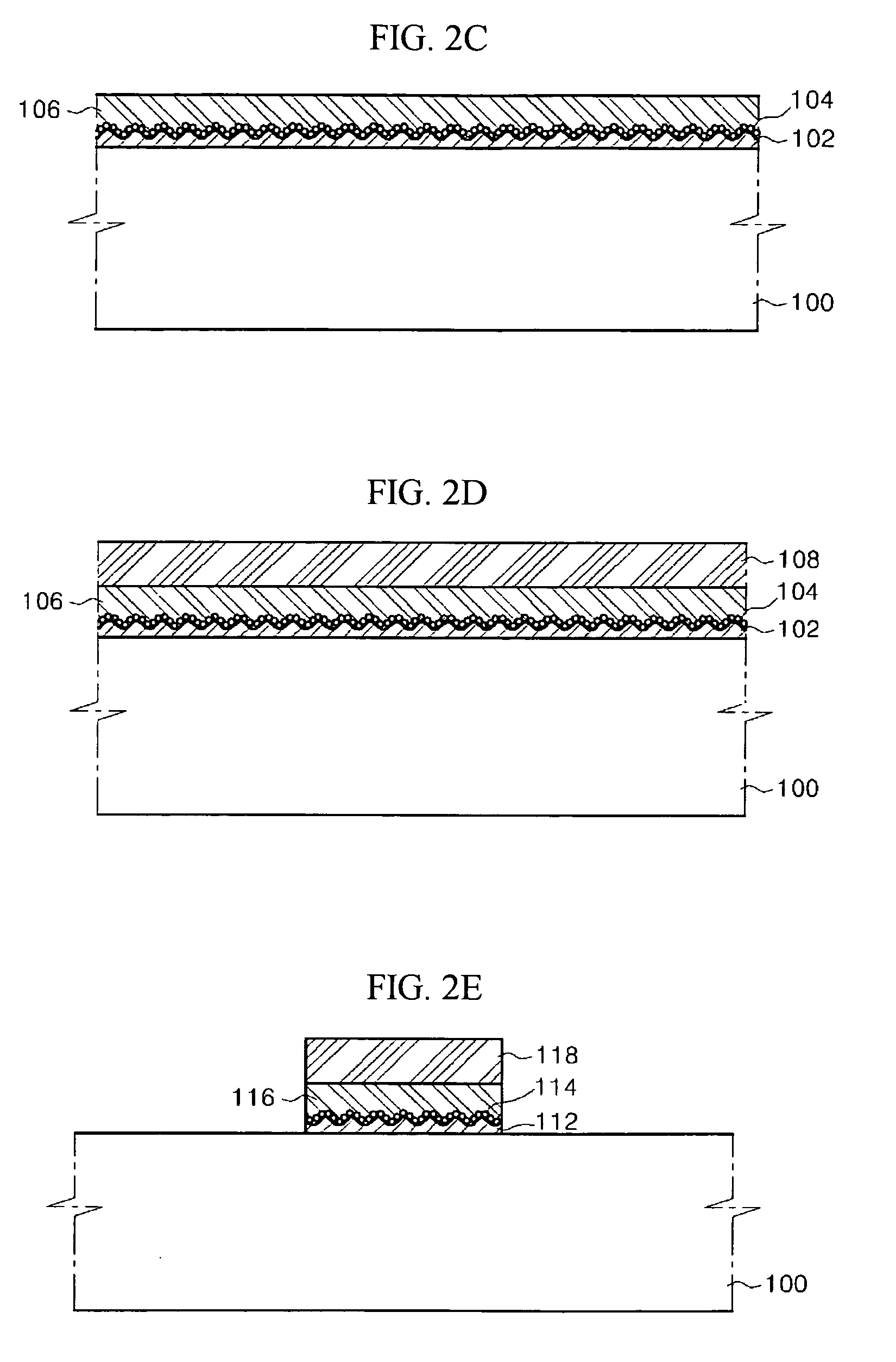
Figure 3
Abstract
Description
[0001] 1. Technical Field
[0002] A method for manufacturing a semiconductor device, which forms a floating gate in a dot shape before the formation of a dual gate of a semiconductor nonvolatile memory device.
[0003] 2. Description of the Related Art
[0004] Generally, floating gates are used for storing charges to erase or delete data in memory devices of a nonvolatile metal oxide semiconductor (MOS) such as read only memories (ROM), erasable programmable read only memories (EPROM) and the like. One such conventional floating gate structure is shown in FIG. 1.
[0005] FIG. 1 is a cross sectional view for explaining a semiconductor device having a floating gate structure according to the prior art.
[0006] First, a tunnel oxide film layer 12, a floating gate oxide film layer 14, a control oxide film layer 16 and a control gate oxide film layer 18 are sequentially formed on a silicon substrate 10. Next, the control gate oxide film layer 18, the control oxide film layer 16, the floating gate o...
Examples
Embodiment Construction
[0013] Hereinafter, preferred embodiments will be described in greater detail in reference to the drawings. In addition, the following embodiments are for illustration only, not intended to limit the scope of this disclosure.
[0014] FIGS. 2a to 2e are cross sectional views showing a method for manufacturing a semiconductor device according to this disclosure.
[0015] First, as shown in FIG. 2a, a tunnel oxide film layer 102 with a rough surface is formed on a silicon substrate 100 having a predetermined substructure. According to a preferred embodiment, the tunnel oxide film layer 102 is formed by depositing SiO.sub.2, which is formed by diffusing oxygen, or a material having a high dielectric constant on the silicon substrate 100.
[0016] Then, as shown in FIG. 2b, a particulate layer or dots or a dotted layer composed of silicon or silicon-germanium are formed on the tunnel oxide film layer 102 for the floating gate layer 104 by chemical mechanical deposition (CVD) with a particle size...