
Method of cleaning etching apparatus
a technology of etching apparatus and cleaning method, which is applied in the direction of cleaning process and apparatus, cleaning using liquids, chemistry apparatus and processes, etc., can solve the problems of reducing the etching performance and occurrence of foreign matter
Patent Information
- Authority / Receiving Office
- US · United States
- Patent Type
- Applications(United States)
- Current Assignee / Owner
- Publication Date
- 2006-08-31
Smart Images
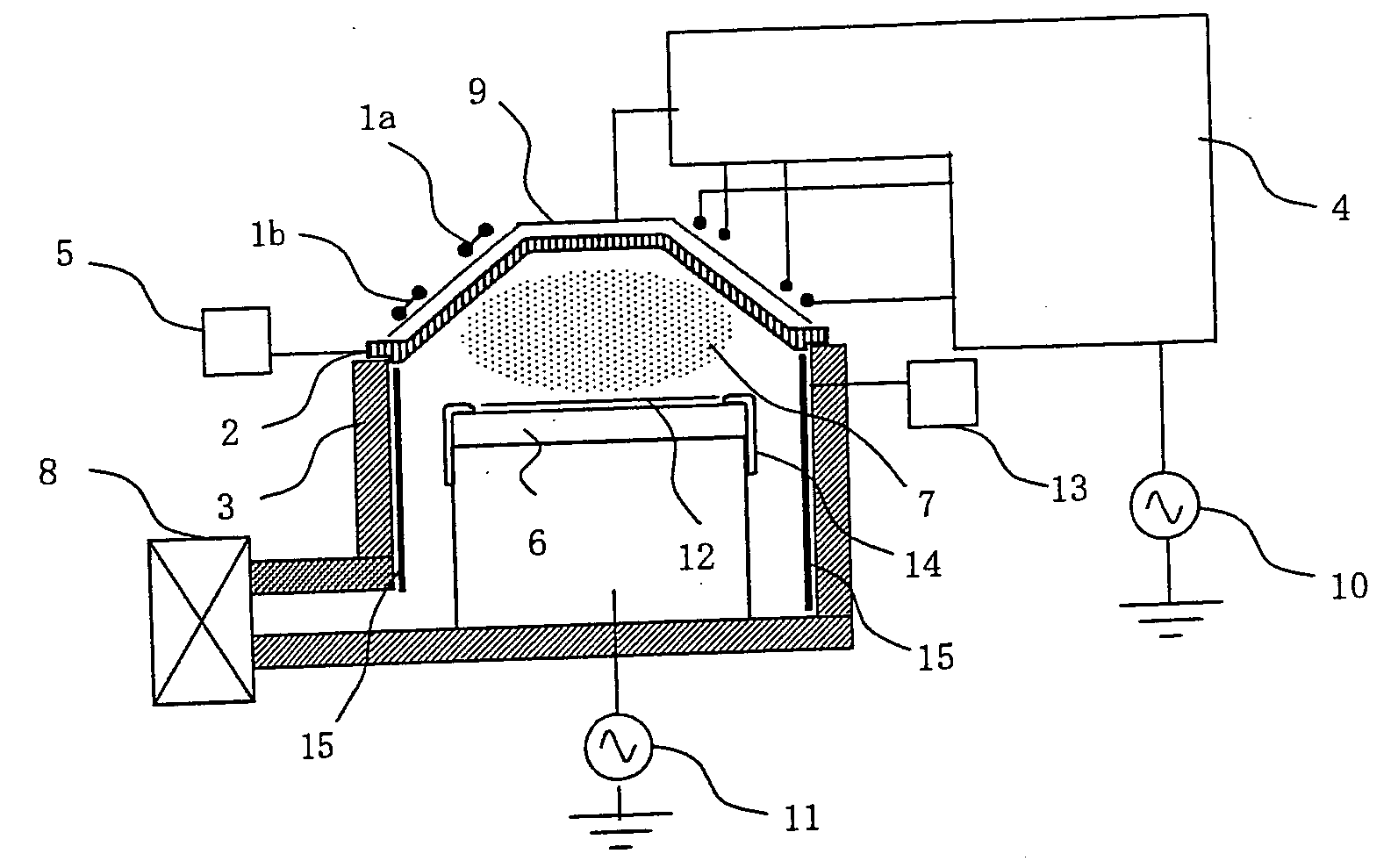
Figure 1 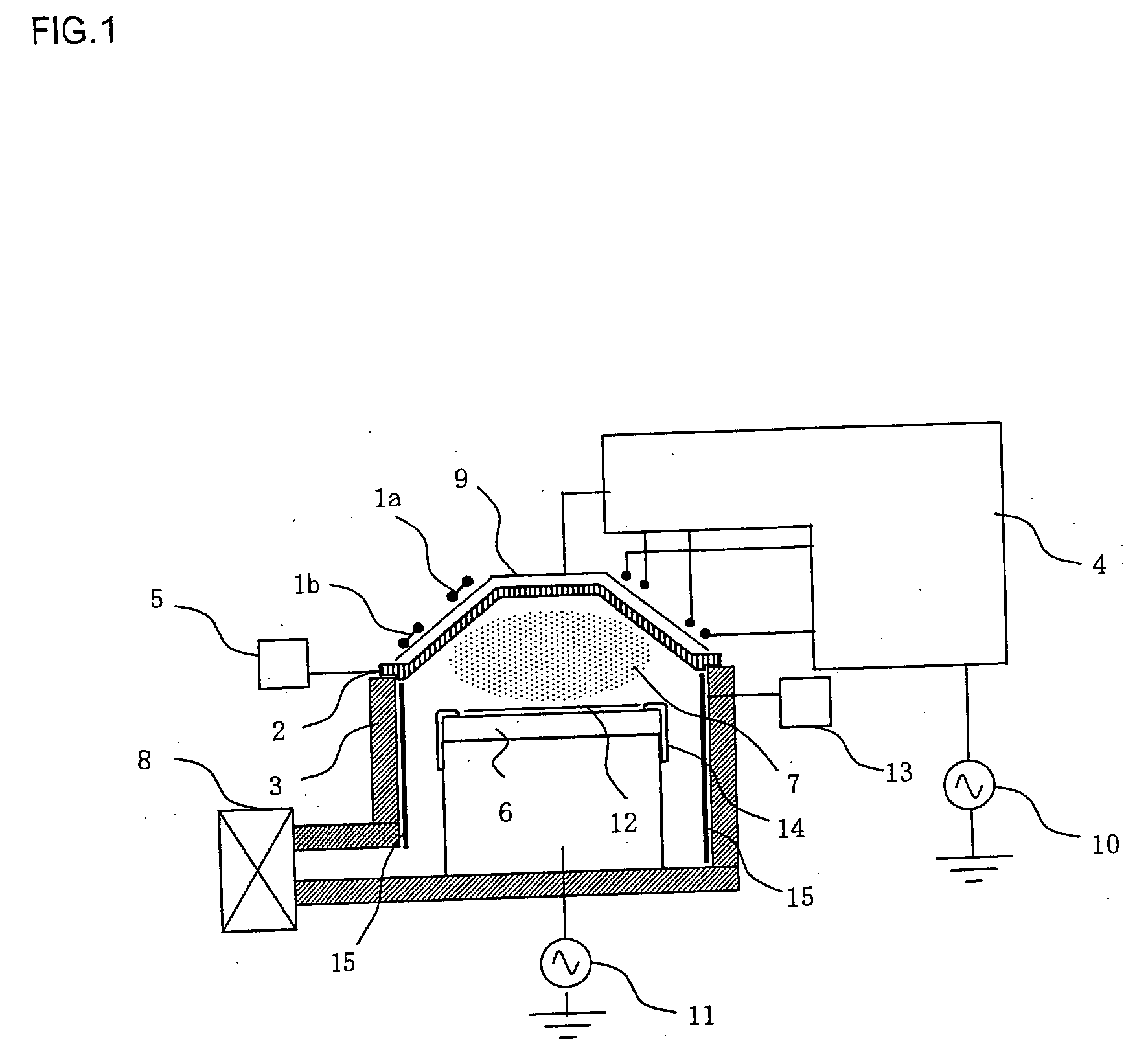
Figure 2 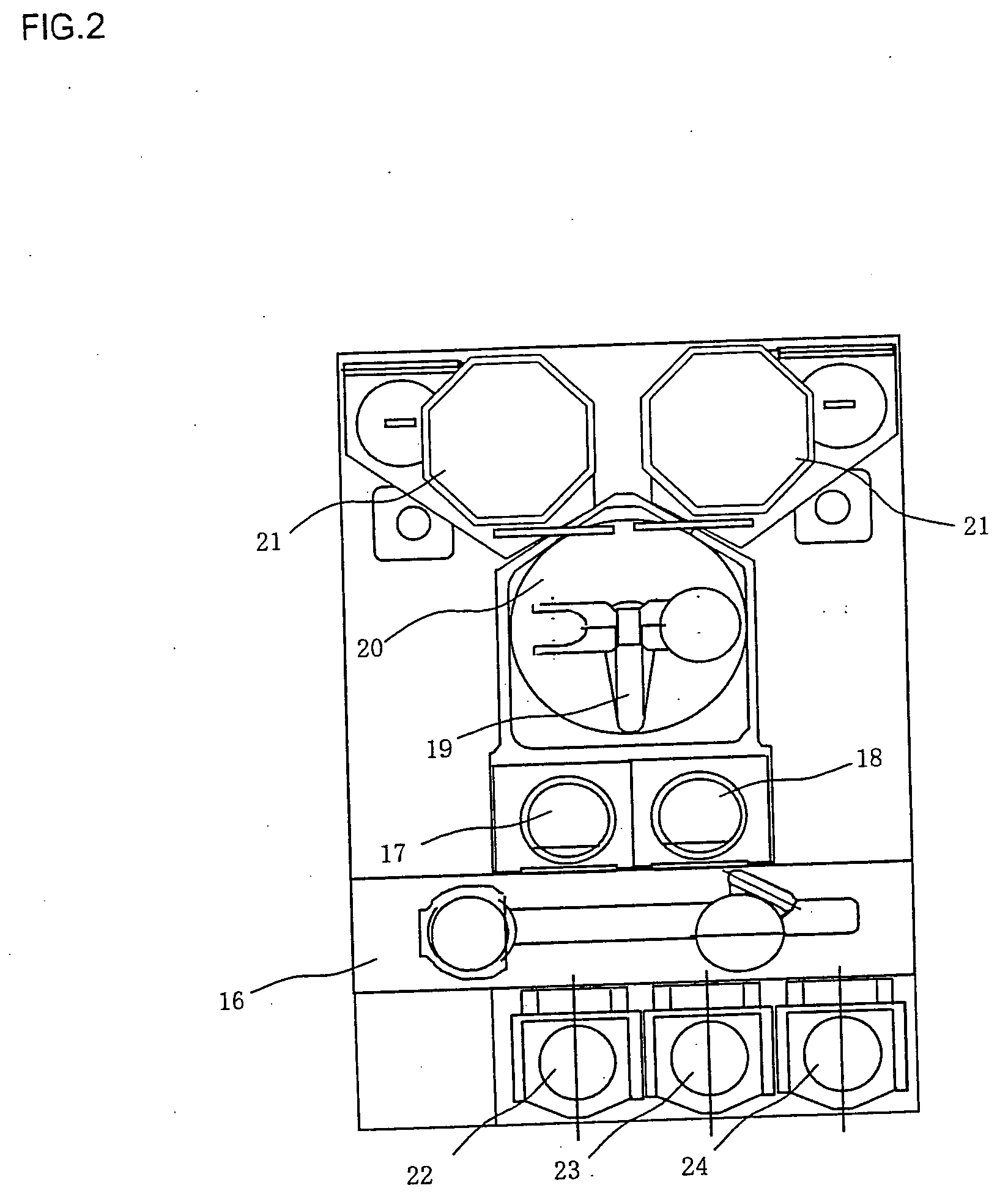
Figure 3
Abstract
Description
[0001] The present application is based on and claims priority of Japanese patent application No. 2005-052434 filed on Feb. 28, 2005, the entire contents of which are hereby incorporated by reference. BACKGROUND OF THE INVENTION
[0002] 1. Field of the Invention
[0003] The present invention relates to a method of cleaning a dry-etching apparatus. In particular, it relates to a cleaning method for an etching apparatus for a semiconductor device, the method being provided to assure that the etching rate of a film to be etched, the in-plane uniformity of etching rate of the film to be etched and the etching rate ratio (selectivity rate) between the film to be etched and a mask material or an underlying material are less variable and reproducible and to keep a stable apparatus condition by minimizing emission of foreign matters in the apparatus.
[0004] 2. Description of the Related Art
[0005] In manufacturing processes of semiconductor devices, etching techniques are used for forming fin...
Examples
Embodiment Construction
[0028] In the following, a method of cleaning a dry etching apparatus according to an embodiment of the present invention will be described with reference to FIGS. 1 to 9 and Tables 1 to 4. The dry etching apparatus used herein to which the cleaning method according to the present invention is applied is an apparatus for etching a workpiece formed on a semiconductor substrate that is supplied with a plasma-forming gas to produce a gas plasma, thereby etching a metal film formed on the substrate. The plasma etching apparatus may be a microwave plasma etching apparatus, an inductively coupled plasma etching apparatus, a helicon plasma etching apparatus, a dual frequency excitation parallel plate plasma etching apparatus.
[0029]FIG. 1 is a cross-sectional view of a plasma etching apparatus used in the present invention. The plasma etching apparatus has a process chamber comprising a discharge section 2 that constitutes a plasma producing section and is made of a non-conductive material...